 GIM
What Is DBC? What Is a DBC Ceramic PCB?
A Complete Guide to Direct Bonded Copper Substrates
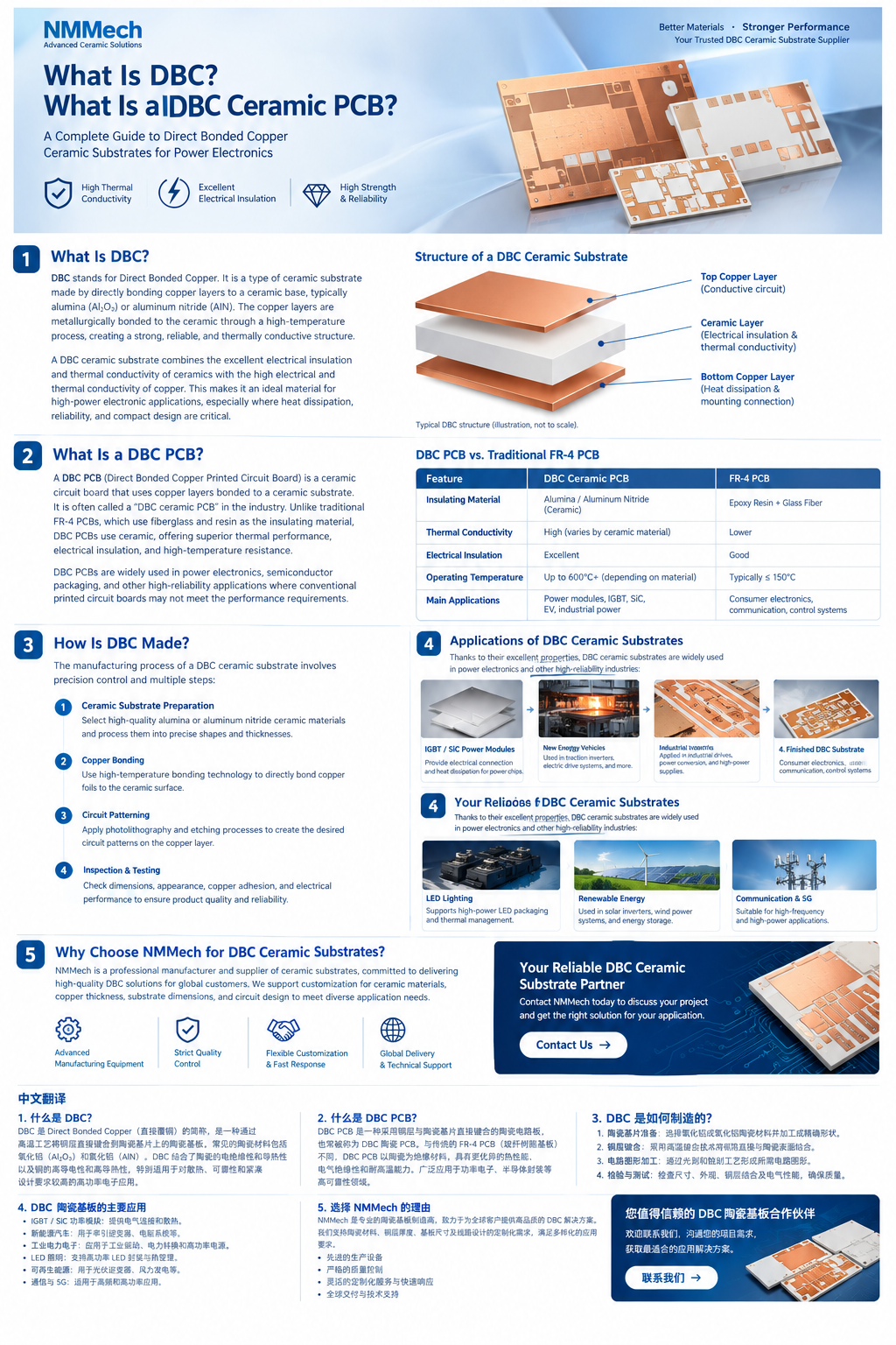
As power electronics continue to evolve, electronic components are expected to handle higher power densities, greater electrical loads, and increasingly demanding thermal conditions. In applications such as electric vehicle inverters, industrial power modules, renewable energy converters, and semiconductor packaging, the choice of substrate can significantly influence thermal management, electrical insulation, and long-term reliability.
This is where DBC (Direct Bonded Copper) ceramic substrates play an important role. By combining copper conductors with an electrically insulating ceramic base, DBC technology provides a practical substrate solution for many high-power electronic applications.
But what exactly is DBC? What is a DBC ceramic PCB, and how does it differ from a conventional printed circuit board? This guide explains the structure, manufacturing process, advantages, applications, and key design considerations of DBC ceramic substrates.
1. What Is DBC?
DBC stands for Direct Bonded Copper. It refers to a ceramic substrate technology in which copper is directly bonded to a ceramic material through a controlled high-temperature process.
A typical DBC substrate consists of a ceramic insulating layer with copper bonded to one or both sides. The copper can subsequently be patterned to form electrical circuits, conductive pads, and heat-spreading areas. Common ceramic materials include aluminum oxide (Al₂O₃), also known as alumina, and aluminum nitride (AlN).
Each material serves a different purpose:
- Copper layer: Provides electrical conductivity, carries current, forms circuit patterns, and helps spread heat across the substrate.
- Ceramic layer: Provides electrical insulation while conducting heat away from power devices toward the cooling structure.
- Bottom copper layer, when used: Can support heat spreading and provide a surface for attachment to a baseplate or cooling assembly.
The main advantage of this structure is that it combines the electrical and thermal properties of copper with the insulating characteristics of ceramic. Unlike bonding systems that rely on a conventional organic adhesive between the copper and ceramic, DBC uses a direct bonding process to establish the interface.
This combination makes DBC particularly useful in power electronics, where high current, heat dissipation, and electrical isolation must be addressed within a compact assembly.
2. What Is a DBC Ceramic PCB?
A DBC ceramic PCB is a circuit carrier made using Direct Bonded Copper technology and a ceramic insulating substrate. It is often called a DBC PCB, DBC ceramic circuit board, or DBC ceramic substrate in commercial and engineering discussions.
Although the term includes “PCB,” a DBC ceramic PCB is different from a conventional FR-4 printed circuit board.
A traditional FR-4 PCB typically uses a glass-fiber-reinforced epoxy laminate as its insulating base. This construction is suitable for many control circuits, communication devices, consumer electronics, and general-purpose electronic products.
A DBC ceramic PCB instead uses ceramic as its insulating layer and directly bonded copper as its conductive layer. This design is particularly valuable when the circuit must manage substantial heat while maintaining electrical isolation.
In many power modules, semiconductor dies are attached to patterned copper areas on the DBC substrate. The ceramic layer electrically isolates the circuit from the underlying cooling structure, while the copper and ceramic work together to transfer heat away from the semiconductor devices.
It is important to understand that DBC is a substrate and metallization technology, not simply a special type of ordinary PCB. Its suitability depends on the electrical, thermal, mechanical, and manufacturing requirements of the final product.
3. How Is a DBC Ceramic Substrate Structured?
The structure of a DBC substrate is relatively simple, but every layer plays an important role in overall performance.
3.1 Top Copper Layer
The top copper layer is generally patterned into the required circuit layout. Depending on the application, it may contain semiconductor attachment areas, conductive paths, bonding pads, and larger copper regions for heat spreading.
Copper thickness affects current-carrying capacity, heat distribution, circuit spacing, and manufacturing feasibility. Thicker copper can be beneficial for high-current applications, but it can also make fine circuit features more difficult to manufacture.
3.2 Ceramic Insulating Layer
The ceramic layer provides electrical insulation between the conductive circuit and the underlying metal baseplate or cooling assembly. It also forms part of the thermal path from the semiconductor device to the heat sink.
Alumina is commonly selected for its balance of cost, electrical insulation, and thermal performance. Aluminum nitride is often considered when higher thermal conductivity is needed.
The choice of ceramic affects thermal resistance, dielectric performance, mechanical strength, thermal expansion, and total substrate cost. The best option depends on the actual design rather than on one material property alone.
3.3 Bottom Copper Layer
Many DBC substrates have copper on both sides of the ceramic. The bottom copper can help distribute heat and provide a conductive surface for attachment to a baseplate or other cooling structure.
Single-sided copper constructions may also be suitable for certain designs. The required configuration depends on the module architecture, electrical requirements, mounting method, and thermal management strategy.
3.4 Surface Finish and Circuit Pattern
After copper bonding, the copper is processed into the required circuit pattern. Depending on the assembly process, a suitable surface finish may be required to support soldering, sintering, or other electrical and mechanical connections.
A DBC substrate should therefore be evaluated as a complete system: ceramic material, ceramic thickness, copper thickness, circuit geometry, surface finish, and the intended attachment method all influence the final result.
4. How Does the DBC Manufacturing Process Work?
DBC manufacturing requires precise process control to achieve a reliable copper-to-ceramic interface and an accurate circuit pattern. A typical production route includes the following stages.
Step 1: Ceramic Substrate Preparation
The process begins with a suitable ceramic base, commonly alumina or aluminum nitride. The ceramic must meet the required specifications for dimensions, thickness, surface condition, and material quality.
Step 2: Copper-to-Ceramic Bonding
Copper foil is bonded directly to the ceramic through a controlled high-temperature process. The conventional DBC process uses a copper-oxygen eutectic mechanism to promote wetting and bonding at the interface.
Temperature control, surface cleanliness, atmosphere, and cooling conditions can affect bond quality. The exact process parameters depend on the materials and production method.
Step 3: Circuit Patterning
Once the copper has been bonded, a circuit pattern is formed using processes such as photolithography and chemical etching. Unwanted copper is removed to create the required conductors, pads, and isolated circuit regions.
Circuit geometry must be designed with the selected copper thickness in mind. Thick copper can influence etching behavior and achievable line widths and clearances, so manufacturing rules should be confirmed before design approval.
Step 4: Surface Treatment and Finishing
Where required, the substrate receives an appropriate surface treatment or finish based on the intended assembly process. Requirements may differ for soldering, semiconductor die attachment, wire bonding, or other connection methods.
Step 5: Inspection and Testing
The finished substrate is inspected against the agreed specifications. Depending on the project, inspection may cover dimensions, circuit geometry, appearance, copper adhesion, flatness, and relevant electrical or reliability requirements.
For demanding applications, quality evaluation should reflect the actual substrate construction and intended operating environment rather than relying on a generic description of DBC technology.
5. What Are the Main Advantages of DBC Ceramic PCBs?
DBC ceramic substrates are widely used because they combine several important properties in one structure.
5.1 Effective Thermal Management
Heat is a major challenge in high-power electronics. Excessive operating temperatures can affect semiconductor performance, component lifetime, and system reliability.
DBC provides a thermal path through the copper and ceramic layers, helping transfer heat away from power devices. The actual thermal performance depends on ceramic selection, layer thicknesses, circuit layout, die attachment, interface materials, and cooling design.
5.2 Electrical Insulation
The ceramic layer electrically separates the copper circuit from the underlying baseplate or cooling structure. This is important in power modules that operate at elevated voltages or contain multiple conductive regions that must remain electrically isolated.
The required insulation performance must be confirmed for the finished design, including ceramic thickness, circuit spacing, operating voltage, and applicable test conditions.
5.3 High Current-Carrying Capability
Copper offers excellent electrical conductivity. By selecting an appropriate copper thickness and conductor geometry, engineers can design DBC circuits for substantial current loads.
However, current capacity is not determined by copper thickness alone. Trace dimensions, operating temperature, thermal resistance, connection design, and cooling conditions must also be considered.
5.4 Reliable Copper-to-Ceramic Bonding
The direct bonding process creates a strong interface between copper and ceramic without a conventional organic adhesive layer between them. This is beneficial in applications where thermal transfer and the integrity of the material interface are important.
Long-term reliability still depends on the complete design, including material selection, copper geometry, assembly quality, mechanical loading, and thermal cycling.
5.5 Compact Power Module Design
By integrating circuit conductors and an electrically insulating ceramic layer, DBC can help simplify the substrate portion of a power module. This supports compact designs where electrical isolation, heat transfer, and current conduction must be achieved within limited space.
5.6 Suitability for Demanding Operating Environments
DBC is commonly considered for applications that experience significant heat generation and repeated operating cycles. The appropriate substrate must nevertheless be selected according to the actual temperature range, voltage requirements, mechanical stresses, and reliability targets.
6. DBC Ceramic PCB vs. Traditional FR-4 PCB
DBC ceramic PCBs and FR-4 PCBs serve different engineering purposes. Neither technology is automatically the best choice for every application.
| Comparison | DBC Ceramic PCB | Traditional FR-4 PCB |
|---|---|---|
| Insulating base | Ceramic, such as Al₂O₃ or AlN | Glass-fiber-reinforced epoxy |
| Conductive layer | Copper directly bonded to ceramic | Copper laminated to the PCB base |
| Thermal management | Well suited to many high-power designs | Depends on board design and thermal management features |
| Electrical insulation | Provided by the ceramic layer | Provided by the FR-4 dielectric |
| Copper thickness | Can support relatively thick copper for power circuits | Varies by PCB specification |
| Typical applications | Power modules, IGBT and SiC devices, inverters | Control circuits, communication devices, consumer electronics |
| Cost considerations | Depends on ceramic, copper, pattern, and specifications | Often economical for general-purpose electronics |
The key distinction is not that DBC replaces FR-4 everywhere. Instead, DBC is designed for applications where ceramic insulation and effective heat transfer are central requirements. FR-4 remains an appropriate and economical choice for many conventional electronic circuits.
7. DBC vs. DPC vs. AMB: What Is the Difference?
DBC is one of several technologies used to create conductive circuits on ceramic substrates. DPC and AMB are two other important options.
DBC — Direct Bonded Copper
DBC uses a controlled high-temperature bonding process to join copper to ceramic. It is widely used in power electronics that require relatively thick copper, electrical insulation, and heat spreading.
DPC — Direct Plated Copper
DPC generally forms copper metallization through deposition and plating processes. It is often selected for applications that require finer circuit features or thinner copper layers, such as certain LED, sensor, RF, and precision electronic components.
AMB — Active Metal Brazing
AMB uses an active-metal brazing process to join copper to ceramic. Silicon nitride is frequently used in AMB substrates for applications requiring high mechanical strength and demanding thermal-cycle performance, including some automotive power modules.
| Technology | General characteristic | Common selection consideration |
|---|---|---|
| DBC | Directly bonded copper on ceramic | Power circuits with relatively thick copper |
| DPC | Deposited and plated copper | Finer circuit features and precision patterns |
| AMB | Active-metal-brazed copper and ceramic | Demanding mechanical and thermal-cycle conditions |
The correct technology depends on circuit geometry, copper thickness, ceramic properties, operating conditions, reliability targets, and manufacturing cost. Engineers should compare complete design requirements rather than choosing a process based on its name alone.
8. What Are the Main Applications of DBC Ceramic Substrates?
DBC substrates are particularly relevant to power electronics and semiconductor packaging.
8.1 IGBT Power Modules
Insulated-gate bipolar transistor (IGBT) modules are used in industrial drives, converters, traction systems, and other high-power equipment. DBC can provide the circuit carrier and ceramic insulation needed to integrate semiconductor devices into a power module.
8.2 SiC Power Electronics
Silicon carbide (SiC) devices support high-efficiency power conversion in many applications. As system designers pursue higher power density and demanding thermal performance, DBC may be considered as part of the substrate and cooling architecture.
8.3 Electric Vehicle Inverters
Electric vehicle traction inverters convert electrical power from the battery into the form needed to drive the motor. Their power modules must address current, voltage, heat dissipation, packaging, and reliability requirements. DBC is one of the substrate technologies used in this field.
8.4 Renewable Energy Systems
Solar inverters, wind power converters, and energy storage systems use power electronics to convert and manage electrical energy. DBC substrates can support power modules in these systems when their thermal and insulation properties fit the design requirements.
8.5 Industrial Power Supplies and Drives
Industrial power supplies, motor drives, welding equipment, and other high-power systems can generate substantial heat during operation. DBC may be selected for power stages where effective heat transfer and electrical isolation are required.
8.6 Other Specialized Applications
Depending on the design, DBC substrates may also be considered for high-power lighting, laser systems, telecommunications power equipment, and other electronic assemblies. Final suitability should be evaluated against the actual electrical, thermal, mechanical, and environmental conditions.
9. How to Choose the Right DBC Ceramic Substrate
Selecting a DBC substrate requires more than identifying a ceramic material. The substrate must be compatible with the complete electronic assembly.
Before requesting a quotation, consider the following parameters:
- Ceramic material: Specify alumina (Al₂O₃), aluminum nitride (AlN), or another material supported by the intended process.
- Ceramic thickness: Define the required thickness based on insulation, thermal performance, mechanical strength, and design constraints.
- Copper thickness: Specify the copper thickness for each side independently, especially for double-sided structures.
- Circuit layout: Provide the latest circuit drawing or manufacturing data, including conductor widths, gaps, pads, and copper-to-edge clearances.
- Substrate dimensions: Confirm the finished outline, dimensional tolerances, and any mounting or cutting requirements.
- Surface finish: Identify the required finish according to the planned soldering, die attachment, wire bonding, or other assembly process.
- Operating conditions: Provide relevant voltage, current, temperature, thermal cycling, and cooling requirements.
- Inspection requirements: Define the critical dimensions, appearance criteria, flatness, adhesion, and electrical tests required for the project.
- Quantity and development stage: Clarify whether the request is for prototypes, engineering validation, pilot production, or volume manufacturing.
Providing complete and consistent information helps suppliers evaluate manufacturability, identify potential design constraints, and quote the appropriate product more accurately.
10. Why Work with NMMech for DBC Ceramic Substrate Solutions?
Choosing a DBC supplier is not only about obtaining a ceramic substrate. It is also about ensuring that the proposed material, copper construction, circuit pattern, and manufacturing process match the needs of the final application.
NMMech focuses on ceramic substrate solutions for power electronics and related industrial applications. Depending on project requirements and confirmed manufacturing capabilities, substrate discussions may cover ceramic material selection, copper thickness, finished dimensions, circuit patterns, and other product specifications.
For engineers, purchasing teams, and electronic component manufacturers, early technical communication can help clarify design details before samples or production orders are arranged.
When contacting NMMech, customers are encouraged to provide the application, technical drawing, ceramic material, copper thickness, required quantity, and any special performance or inspection requirements. This information provides a clearer basis for discussing feasibility and selecting an appropriate solution.
11. Frequently Asked Questions About DBC
What does DBC stand for?
DBC stands for Direct Bonded Copper. It describes a process for directly bonding copper to a ceramic substrate.
What is a DBC ceramic PCB?
A DBC ceramic PCB is a ceramic circuit carrier that uses directly bonded copper to form conductive patterns. It is commonly used in power electronics and semiconductor packaging.
Is DBC the same as a conventional PCB?
No. DBC uses a ceramic insulating base and directly bonded copper, while conventional FR-4 PCBs typically use a glass-fiber-reinforced epoxy laminate. The two technologies serve different application requirements.
Which ceramic materials are used in DBC substrates?
Alumina (Al₂O₃) and aluminum nitride (AlN) are common options. Their thermal, electrical, mechanical, and cost characteristics differ, so selection should be based on the application.
What is the difference between DBC and DCB?
DBC and DCB are both commonly used abbreviations for direct copper bonding technology in ceramic substrates. Terminology may vary among suppliers and technical documents.
Can DBC substrates be customized?
DBC substrates can be specified according to project requirements, subject to the supplier’s available processes and manufacturing limits. Common discussion points include ceramic material, copper thickness, substrate dimensions, circuit pattern, and inspection criteria.
What information is needed to request a DBC quotation?
A useful inquiry typically includes the technical drawing, ceramic material, ceramic thickness, copper thickness on each side, finished dimensions, surface finish, quantity, application, and relevant performance requirements.
Conclusion: DBC Is an Important Substrate Technology for Power Electronics
DBC ceramic substrates combine conductive copper with an electrically insulating ceramic base, making them an important option for power modules and other electronic assemblies that require effective heat transfer and electrical isolation.
Understanding the structure, manufacturing process, material choices, and design constraints of DBC helps engineers and purchasing teams make better-informed decisions. The right solution should be evaluated against the complete application, including current, voltage, thermal management, mechanical requirements, assembly process, and reliability targets.
Looking for a DBC ceramic substrate solution for your project? Contact NMMech with your drawing and technical requirements to discuss material options, copper construction, circuit design, and manufacturing feasibility.