 GIM



High-Temperature Co-Fired Ceramics (HTCC):
The Foundational Material Backbone for High-Reliability Electronic Packaging
Executive Summary
As global power consumption in next-generation microelectronics escalates rapidly, advanced electronic systems face an interconnected triad of physical constraints: aggressive thermal dissipation requirements, stringent hermetic sealing mandates, and ultra-long-term operational reliability [1]. High-Temperature Co-Fired Ceramic (HTCC) packaging—specifically Aluminum Nitride (AlN)-based substrates—has emerged as the definitive technical foundation to overcome the thermal and physical boundaries of traditional organic and metallic packaging materials [2].
1. The Thermal and Mechanical Imperative in Modern Packaging
In cutting-edge optoelectronic systems, such as 800G and 1.6T optical transceivers, single-module power consumption now routinely exceeds 45 Watts [3]. To prevent thermal degradation and optical phase distortion, laser diode junction temperatures must be maintained strictly below 60°C [4].
Traditional organic substrates (such as FR-4 and BT resin) and basic metal packages fail to deliver the requisite thermal conductivity and dimensional stability under extreme operating cycles [5]. HTCC technology solves this challenge through a monolithic ceramic-metal structure created by co-firing refractory metals with high-purity ceramic substrates [6].
Key Physical & Material Properties of AlN-HTCC:
- Thermal Conductivity: 170–200 W/(m·K), ensuring low thermal resistance and ultra-fast heat spreader performance.
- Coefficient of Thermal Expansion (CTE): 4.5–5.0 ppm/°C, matching Silicon (Si), Gallium Nitride (GaN), and Indium Phosphide (InP) chips to prevent micro-cracking and thermal-stress delamination.
- Hermetic Integrity: Fully inorganic vacuum-tight seal achieving 10-9 atm·cm³/s leak rates, guaranteeing a 20+ year mission-critical operational lifespan.
2. Next-Generation Application Paradigms
2.1 Optical Communications & Co-Packaged Optics (CPO)

Modern optical transceivers operating from 2.5 Gbps to 800 Gbps depend heavily on multi-layer ceramic shells to preserve high-frequency signal integrity and suppress high-speed electromagnetic interference [7]. In Co-Packaged Optics (CPO) architectures, where silicon photonics dies are co-located with high-speed compute ASICs, substrates must satisfy a rigorous Five-Dimensional Performance Framework including high-frequency signal stability, high-density routing, and vacuum-grade hermetic sealing.
2.2 Wide Bandgap (WBG) Power Semiconductors
 Silicon Carbide (SiC) and Gallium Nitride (GaN) power switches operate at vastly higher junction temperatures, switching frequencies, and voltage gradients than legacy silicon devices. AlN-HTCC serves as an unyielding structural chassis, simultaneously acting as an electrical isolator and a primary thermal conduction pathway that resists extreme electrical breakdown and thermal cycling fatigue.
2.3 Automotive & Harsh-Environment Electronics
 Sensors and power control modules installed in electric vehicles (EVs) and autonomous systems must satisfy stringent AEC-Q200 qualification standards [8]. LiDar transceiver units, traction inverters, and engine control units rely on HTCC packaging due to its exceptional mechanical shock resistance and stable performance across ambient temperature sweeps ranging from -55°C to +200°C.
2.4 Advanced Packaging & Hybrid Heterogeneous Integration
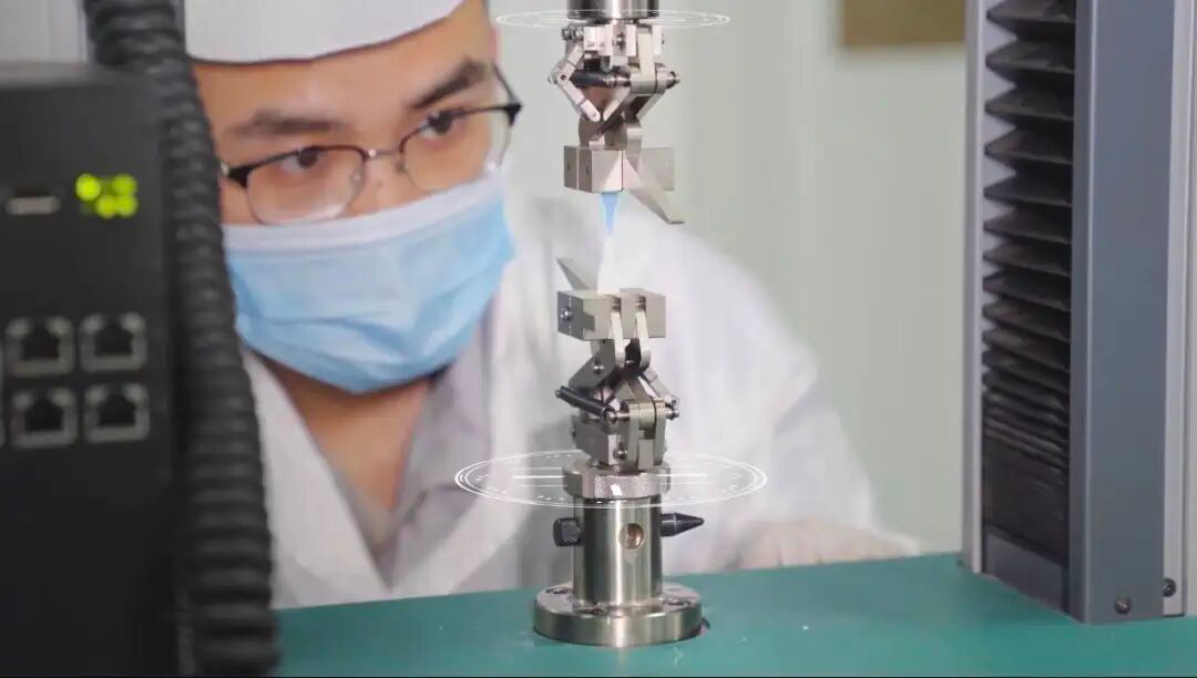 To mitigate warp and stress in ultra-large-area multi-chip modules (MCM), advanced packaging architectures utilize an AlN Ceramic Core combined with Organic Build-up Layers. This hybrid core design provides mechanical stiffness and precise planar stability, unlocking reliable fine-pitch routing for 2.5D/3D heterogeneous integration.
3. The NMM Technology Platform: Advanced Manufacturing Capabilities
The NMM Power Semiconductor Research Institute has established a world-class AlN Multi-Layer Co-Firing platform engineered to supply precision substrates for high-reliability industries.
| Technical Parameter | NMM AlN-HTCC Benchmark Standard | Industry Baseline |
|---|---|---|
| Thermal Conductivity | ≥ 170 W/(m·K) | 130 ~ 150 W/(m·K) |
| Flexural Strength | ≥ 350 MPa | 280 ~ 300 MPa |
| Surface Roughness (Ra) | ≤ 0.05 μm | 0.1 ~ 0.2 μm |
| Routing Pitch Capability | 50 μm Fine-Line | 100 μm |
| Layer Stack Capability | > 20 Layers High-Density Routing | 8 ~ 12 Layers |
Active R&D Frontiers:
- Ultra-High Thermal Composite Materials: Pushing thermal conductivity bounds past 230 W/(m·K).
- Sub-50μm Fine Trace Lithography: Enabling dense micro-via and line/space geometries.
- Mass Production Scale-Up: Standardized batch firing processes for high-yield, large-format ceramic panels.
4. Conclusion & Strategic Partner Collaboration
From high-temperature atmospheric sintering to scalable thermal management systems in AI data centers, HTCC ceramics are transitioning from passive housings to active system-enabling platforms.
We invite global tier-1 system integrators, semiconductor packaging engineers, and technology partners to collaborate with NMM on custom design, co-development, and qualification testing for next-generation ceramic packaging solutions.
Authoritative Industry & Academic References
- SEMI (Semiconductor Equipment and Materials International)
Global industry association providing international standards and market intelligence for microelectronics and advanced semiconductor packaging.
https://www.semi.org - IMEC (Interuniversity Microelectronics Centre)
World-leading research and innovation hub in nanoelectronics, 3D packaging technologies, and advanced substrate materials.
https://www.imec-int.com - IEEE Xplore Electronics Packaging Society
Leading peer-reviewed technical repository for research papers on high-frequency ceramics, thermal management, and HTCC packaging.
https://www.ieee.org - Optica (formerly Optical Society of America – OSA)
The premier global authority for optics and photonics, detailing optical transceiver integration and Co-Packaged Optics (CPO) standards.
https://optica.org - ScienceDirect (Ceramics & Packaging Materials Database)
Comprehensive scientific reference on Aluminum Nitride (AlN) physical properties, thermal conductivity, and co-firing mechanics.
https://www.sciencedirect.com - NIST (National Institute of Standards and Technology)
U.S. government standards institute providing benchmark data on ceramic material characterization, thermal expansion, and mechanical testing.
https://www.nist.gov - IEEE Power Electronics Society (PELS)
Technical authority focused on Wide Bandgap (SiC/GaN) power semiconductors and high-reliability thermal substrate design.
https://www.ieee-pels.org - AEC (Automotive Electronics Council)
Official organization establishing AEC-Q200 stress test qualification standards for passive ceramic components in automotive electronics.
http://www.aecouncil.com - JEDEC Solid State Technology Association
Global leader in developing open standards and reliability specifications for the microelectronics and semiconductor packaging industry.
https://www.jedec.org - ASM International (The Materials Information Society)
Authority on engineered materials, technical ceramics, refractory metals (W, Mo, Mo-Mn), and high-temperature metallurgy.
https://www.asminternational.org