 GIM


Power Electronic Substrates: How DBC, DPC and AMB Ceramic Substrates Enable Advanced Power Electronics
Category: News & Insights |
Power Electronics | Advanced Materials
conductive circuits and thermal management for advanced
electronic systems.
Introduction: The Foundation of Reliable Power Electronics
As power electronics continue to evolve, manufacturers face
increasingly demanding requirements for thermal management,
electrical insulation, mechanical reliability and compact
system design. Electric vehicles, renewable energy systems,
industrial motor drives, high-power converters and advanced
lighting equipment all depend on electronic components that
can operate reliably under demanding electrical and thermal
conditions.
At the heart of many of these systems are
power electronic substrates. Unlike
conventional printed circuit boards designed primarily for
signal transmission and general electronic interconnection,
ceramic power substrates are engineered to provide electrical
insulation while supporting heat transfer and reliable
electrical connections for power semiconductor devices.
Direct Bonded Copper (DBC), Direct Plated Copper (DPC) and
Active Metal Brazed (AMB) substrates are three important
technologies used in advanced electronic packaging. Although
all three combine ceramic insulation with conductive metal,
their manufacturing processes, material characteristics and
ideal applications differ.
Understanding these differences helps engineers and
procurement teams select substrate solutions that match
their electrical, thermal, mechanical and manufacturing
requirements. For manufacturers developing power modules,
semiconductor packages and high-reliability electronic
assemblies, selecting the right ceramic substrate is an
essential step toward improving product performance and
long-term reliability.
 1. What Are Power Electronic Substrates?
 1. What Are Power Electronic Substrates?
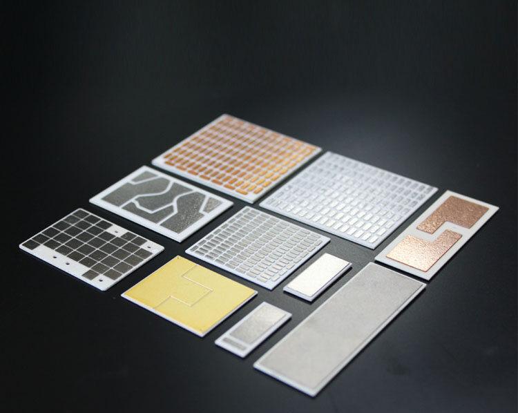
A power electronic substrate is a functional component that
supports semiconductor devices and provides an electrically
insulating foundation for conductive circuit patterns.
In many power module designs, the substrate also forms an
important part of the thermal pathway between semiconductor
chips and the cooling system.
A typical ceramic power substrate consists of three main elements:
- Ceramic insulation layer:
Provides electrical isolation and contributes to thermal
management and mechanical stability. - Metal circuit layer:
Usually copper or another specified conductor, designed to
carry current and provide mounting areas for semiconductor
components. - Interface and surface finish:
Supports bonding, soldering, component attachment and
compatibility with downstream assembly processes.
The selection of ceramic material, metal thickness, substrate
dimensions, circuit geometry and surface treatment can
significantly influence the performance of the finished
assembly.
Common ceramic materials include alumina (Al2O3),
aluminum nitride (AlN) and silicon nitride (Si3N4).
Each offers a different balance of thermal conductivity,
electrical insulation, mechanical strength, thermal expansion
and cost.
The appropriate substrate depends not only on the properties
of an individual material but also on the operating conditions
of the complete power module.
 2. DBC Substrates: Efficient Thermal Management and Electrical Insulation
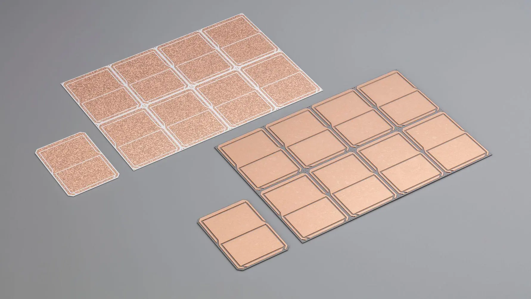 2. DBC Substrates: Efficient Thermal Management and Electrical Insulation
with patterned copper circuits for power electronic modules.
What Is DBC Technology?
Direct Bonded Copper (DBC), also commonly referred to as
Direct Bond Copper, is a technology that bonds copper directly
to a ceramic substrate through a controlled high-temperature
process. The copper layer can subsequently be patterned to
form the required electrical circuits.
Depending on the design, DBC substrates can use alumina or
aluminum nitride ceramic. The resulting structure combines
a ceramic insulation layer with conductive copper surfaces,
making it suitable for many power semiconductor applications.
Key Characteristics of DBC Substrates
Efficient heat transfer:
Heat generated by power semiconductor devices must be
transferred away from sensitive components. DBC substrates
provide a thermal pathway through the ceramic layer and
toward the module’s cooling structure. Actual thermal
performance depends on ceramic composition, thickness,
copper geometry, interface materials and overall module design.
Electrical insulation:
The ceramic layer separates conductive circuit areas from
underlying structures where electrical isolation is required.
Insulation performance must be evaluated against operating
voltage, dielectric requirements, creepage distance and
clearance requirements.
Copper circuit flexibility:
The copper surface can be patterned to accommodate different
component layouts, current paths and interconnection
requirements. This allows engineers to design substrate
circuits for specific power module architectures.
Established manufacturing technology:
DBC is a well-established substrate technology for power
electronics. It can be suitable for industrial power modules,
power conversion systems and applications requiring a
practical balance of thermal performance, electrical
insulation and manufacturing cost.
Typical Applications of DBC Substrates
- IGBT and other power semiconductor modules
- Industrial power supplies and power converters
- Motor drives and inverter systems
- Renewable energy conversion equipment
- LED modules and selected high-power lighting systems
- Automotive electronic assemblies, subject to design and qualification requirements
For applications requiring dependable electrical insulation,
effective heat transfer and patterned copper circuits,
DBC remains an important option for substrate design.
3. DPC Substrates: Precision Copper Patterns for Advanced Packaging
selected ceramic electronic packaging applications.
What Is DPC Technology?
Direct Plated Copper (DPC) is a ceramic metallization
technology in which copper is deposited onto a ceramic
surface through plating-related processes. The process can
support precise circuit pattern formation and is particularly
relevant to applications requiring fine features and
controlled metallization.
DPC substrates are used where circuit geometry, conductor
definition and compatibility with advanced electronic
packaging processes are important considerations.
Achievable feature size, copper thickness, dimensional
tolerance and surface finish depend on the manufacturing
process, ceramic material, design rules and required
production specifications.
Key Advantages of DPC Substrates
- Fine circuit pattern capability:
Supports precise copper patterns for compact electronic
designs and carefully defined electrical paths. - Design flexibility:
Circuit layouts can be developed according to application
requirements, including conductor width, spacing, contact
areas and component mounting arrangements. - Ceramic-based packaging compatibility:
Combines a ceramic insulating body with patterned copper
metallization for selected optoelectronic and electronic
packaging applications. - Potential for compact integration:
May be suitable for systems where component density and
package dimensions are important.
Typical Applications of DPC Substrates
- High-power LED and optoelectronic packaging
- Laser diode and optical communication components
- Selected RF and high-frequency electronic assemblies
- LiDAR and precision optoelectronic modules
- Ceramic circuit substrates for compact electronic packages
DPC should not automatically be regarded as a replacement
for DBC or AMB. Its suitability depends on copper thickness,
circuit geometry, thermal load, mechanical conditions and
assembly requirements. Engineers should confirm the actual
design rules and performance data with the substrate
manufacturer before finalizing the package architecture.
4. AMB Substrates: Reliability for Demanding Power Module Applications
demanding thermal and mechanical operating conditions.
What Is AMB Technology?
Active Metal Brazed (AMB) is a substrate manufacturing
technology that uses an active-metal brazing process to join
conductive metal, commonly copper, to ceramic materials.
Aluminum nitride and silicon nitride are used in AMB substrate
designs, depending on the application and product specification.
AMB is particularly relevant to power electronics that
experience demanding thermal cycling, mechanical stress and
high power density. The ceramic material and bonding
structure are selected to meet the requirements of the
complete power module.
Silicon nitride AMB substrates are especially important in
applications where mechanical strength and resistance to
thermal-mechanical stress are key design considerations.
Key Characteristics of AMB Substrates
- Mechanical reliability:
Substrates must withstand stresses generated by temperature
changes, differences in thermal expansion and repeated
operating cycles. - Thermal management:
AMB substrates combine conductive metal with ceramic
insulation to support heat transfer away from semiconductor
devices. - Electrical insulation:
The ceramic layer provides isolation, while the metal layer
forms the circuit and component attachment areas. - Demanding operating environments:
AMB is often considered for power modules exposed to
substantial thermal and mechanical loading.
Typical Applications of AMB Substrates
- Electric vehicle and hybrid vehicle power modules
- Traction inverters and railway power conversion systems
- High-power industrial drives
- Renewable energy inverters and power conversion equipment
- High-reliability power semiconductor assemblies
Engineers should evaluate temperature range, thermal cycling,
mechanical loading, power density and expected service life
when selecting AMB substrates.
 5. DBC vs. DPC vs. AMB: How to Choose the Right Substrate
 5. DBC vs. DPC vs. AMB: How to Choose the Right Substrate
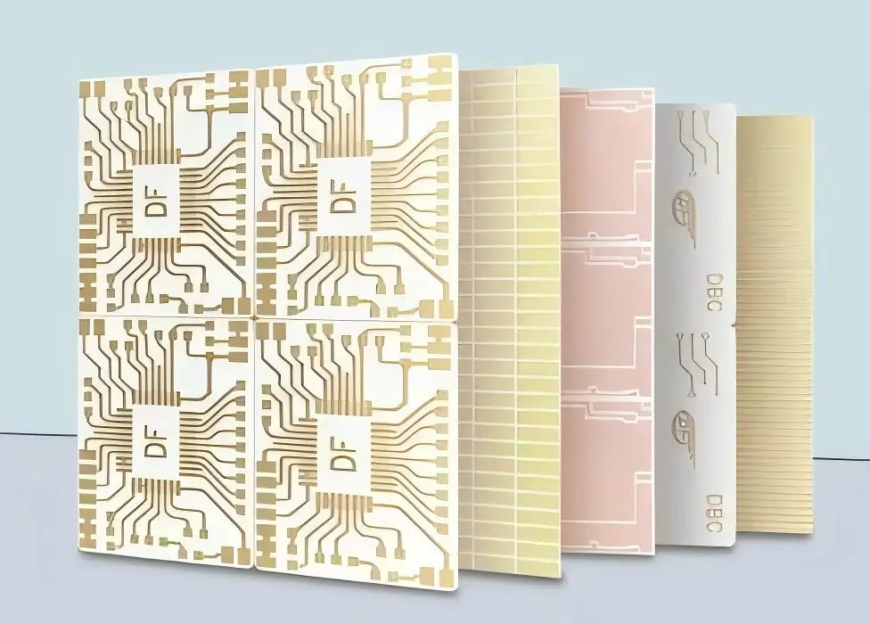
There is no single substrate technology that is best for
every application. The right selection depends on the
technical requirements of the product, the intended
operating environment and the manufacturing process.
| Selection Factor | DBC | DPC | AMB |
|---|---|---|---|
| Manufacturing Principle | Direct copper bonding | Copper plating and metallization | Active-metal brazing |
| Main Design Focus | Balanced thermal and electrical performance | Precision copper patterning | Reliability under demanding operating conditions |
| Common Ceramic Options | Alumina, AlN | Depends on the process | AlN, Si3N4 |
| Circuit Design | Patterned copper circuits | Precision patterned copper | Patterned metal circuits |
| Typical Applications | Power modules, converters, industrial electronics | LED, optoelectronics, precision packages | EV power modules, traction and high-reliability power electronics |
| Key Evaluation Criteria | Thermal performance, insulation, copper geometry and cost | Feature size, metallization, surface finish and packaging requirements | Mechanical stress, thermal cycling, insulation and reliability |
Note: This table provides general technology guidance.
Actual capabilities and material combinations vary by
manufacturer and product design. Verify technical
specifications before making a final selection.
A Practical Selection Process
- Define electrical requirements.
Identify operating voltage, current, insulation
requirements and circuit layout. - Evaluate thermal conditions.
Determine heat load, operating temperature range, cooling
method and acceptable thermal resistance. - Assess mechanical stresses.
Consider thermal cycling, vibration, mounting conditions,
substrate dimensions and differences in thermal expansion. - Select ceramic and metal configurations.
Compare alumina, aluminum nitride and silicon nitride,
together with suitable copper thickness and surface finish. - Confirm manufacturability.
Review circuit spacing, copper pattern dimensions,
tolerances, substrate thickness and assembly requirements. - Validate the design.
Conduct prototype evaluation and application-specific
testing where necessary before volume production.
A structured selection process can help reduce redesign risk,
improve manufacturability and align substrate performance
with the requirements of the final product.
6. Key Applications Driving Demand for Ceramic Power Substrates
electrical insulation in advanced power conversion systems.
Electric Vehicles and Automotive Power Electronics
Electric vehicles rely on power electronics to manage energy
conversion between the battery, motor and supporting
electrical systems. Inverters, converters and other power
modules must balance electrical performance, thermal
management, compact packaging and long-term reliability.
DBC and AMB substrates may be selected according to the
power module architecture, ceramic material,
thermal-mechanical loading and qualification requirements.
The final design must also satisfy applicable automotive
reliability and manufacturing standards.
Renewable Energy Systems
Solar inverters, energy storage converters and wind power
conversion systems use power semiconductor devices to manage
electrical energy efficiently. Ceramic substrates support
these devices by combining conductive circuits with
electrical insulation and a thermal pathway.
Selection depends on power rating, operating environment,
cooling architecture and expected service conditions.
Industrial Automation and Motor Drives
Industrial power supplies, variable-frequency drives, servo
systems and motor controllers require stable power conversion
and effective heat management. DBC substrates can be suitable
for many conventional power module designs, while AMB may be
evaluated when more demanding mechanical or thermal-cycling
requirements apply.
LED and Optoelectronic Systems
High-power LEDs, laser diodes and selected optical
communication components can generate substantial heat
within compact packages. DPC or other ceramic metallization
technologies may be appropriate when precise circuit
patterns and controlled component mounting are required.
Selection must consider thermal resistance, electrical
design, package dimensions, optical requirements and
assembly compatibility.
Railway and High-Power Conversion Equipment
Railway traction systems and high-power industrial
converters can expose power modules to demanding thermal
and mechanical conditions. Substrate design is therefore
an important part of the overall reliability strategy.
AMB substrates based on suitable ceramic materials may be
considered where the application requires a combination
of electrical insulation, heat transfer and mechanical
robustness.
7. Material Selection: Alumina, Aluminum Nitride and Silicon Nitride
Ceramic selection is one of the most important decisions
in substrate engineering. Different ceramics offer
different combinations of thermal, electrical and
mechanical properties.
Alumina (Al2O3)
Alumina is widely used in electronic substrates because of
its established manufacturing processes, electrical
insulation characteristics and cost-effective material
options. It is frequently considered for industrial
electronics, power modules and applications where a
balanced performance-to-cost ratio is important.
Aluminum Nitride (AlN)
Aluminum nitride is known for its relatively high thermal
conductivity compared with conventional alumina grades.
It may be appropriate for designs with demanding heat-transfer
requirements, provided the mechanical, electrical and
manufacturing specifications are also satisfied.
Silicon Nitride (Si3N4)
Silicon nitride is valued for its mechanical strength and
fracture toughness among advanced engineering ceramics.
It is often evaluated for power module designs exposed to
substantial thermal-mechanical stress, particularly when
used in suitable AMB constructions.
Material properties vary by grade, composition, porosity,
manufacturing process and test method. Buyers should
request the manufacturer’s current technical data sheet
rather than relying on generic material values.
8. Quality Control and Custom Manufacturing Considerations
The performance of a ceramic power substrate depends on
more than the ceramic material alone. Bonding quality,
copper geometry, surface condition, dimensional accuracy
and process consistency can all affect the finished product.
When evaluating a substrate supplier, consider the following:
- Material traceability:
Confirm ceramic grade, metal specifications and
material documentation. - Bonding integrity:
Evaluate the bonding interface and its suitability for
intended thermal and mechanical conditions. - Circuit geometry:
Confirm conductor width, spacing, edge definition and
dimensional tolerances. - Surface finish:
Select appropriate treatment for soldering, wire bonding,
plating or other assembly requirements. - Electrical performance:
Verify insulation and dielectric requirements for the
intended operating conditions. - Thermal and mechanical reliability:
Determine whether application-specific cycling, strength
or other qualification tests are required. - Production consistency:
Confirm process controls, inspection criteria, sampling
plans and batch traceability.
Testing methods and acceptance criteria should be agreed
upon according to the application, customer drawings and
applicable standards. No single inspection result can
independently guarantee the reliability of a complete
power module.
From Prototype to Production
Early communication between the substrate manufacturer,
module designer and assembly team can help identify
technical risks before production tooling and downstream
processes are finalized.
For customized projects, establish the following information at the quotation stage:
- Ceramic material and substrate thickness
- Copper thickness on each side
- Circuit drawings and dimensional tolerances
- Required surface treatment
- Expected electrical, thermal and mechanical conditions
- Prototype quantity and anticipated production volume
- Inspection requirements and applicable qualification standards
Clear technical specifications help the supplier assess
manufacturability, provide a more accurate quotation and
reduce unnecessary design iterations.
 9. Customized Ceramic Substrate Solutions from NMMech
 9. Customized Ceramic Substrate Solutions from NMMech
NMMech focuses on advanced materials and electronic
substrate solutions, including ceramic substrates and
copper-clad substrate technologies for industrial and
electronic applications.
For engineers developing new products or optimizing
existing power modules, substrate selection should be
based on the specific combination of thermal management,
electrical insulation, circuit layout, mechanical loading
and manufacturing requirements.
Depending on project scope and confirmed manufacturing
capabilities, customized substrate development may involve
material selection, copper pattern design, dimensional
requirements, surface treatment and prototype evaluation.
Our recommended approach is to begin with the customer’s
application and technical drawings, identify the most
important performance requirements, and evaluate suitable
substrate structures against the intended operating
conditions.
Whether the project involves a new semiconductor package,
an industrial power module or a specialized ceramic circuit,
early technical communication helps establish a practical
path from initial design to validated production.
For accurate evaluation, customers are encouraged to provide
available drawings, material preferences, copper thickness
requirements, operating conditions and estimated order
quantities.
Conclusion: Choosing the Right Foundation for Power Electronics
DBC, DPC and AMB ceramic substrates each serve important
roles in modern electronic packaging. DBC offers an
established approach for many power electronic designs,
DPC supports applications that benefit from precision
copper metallization, and AMB is an important option for
power modules facing demanding thermal-mechanical conditions.
The best solution is not determined by one specification
alone. Ceramic composition, copper configuration, circuit
geometry, thermal performance, electrical insulation,
mechanical reliability and manufacturing capability must
be considered together.
By matching substrate technology to actual application
requirements, engineers can develop more reliable power
modules, improve thermal management and support the
long-term performance of advanced electronic systems.
Looking for a Customized Ceramic Substrate Solution?
Contact NMMech with your technical drawings, material
requirements and application details to discuss DBC, DPC
or AMB substrate options, prototype evaluation and
potential production requirements.
Contact NMMech for Technical Consultation
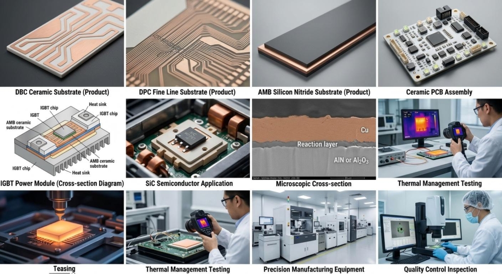
Technical Resources for Ceramic Substrates and Power Electronics
Explore selected international standards organizations, scientific
research institutions, and academic resources covering ceramic
substrates, electronic packaging, thermal management, PCB technology,
and power electronics reliability.
1. International Standards and Technical Organizations
International Electrotechnical Commission (IEC)
International electrotechnical standards and technical information
relevant to electrical equipment, electronic components, and safety.
Institute of Electrical and Electronics Engineers (IEEE)
A global professional organization supporting research and knowledge
exchange in electrical engineering, electronics, and semiconductor
technologies.
SEMI
Industry information and technical initiatives related to
semiconductor manufacturing, electronics, and advanced technologies.
2. Scientific Research and Academic Publications
IEEE Xplore Digital Library
Research papers and technical publications on power electronics,
semiconductor devices, thermal management, and electronic systems.
ScienceDirect
A scientific literature platform covering materials science,
ceramics, electronics, engineering, and reliability research.
SpringerLink
Academic books and research articles covering advanced materials,
ceramic engineering, electronic packaging, and applied physics.
Google Scholar
A search resource for scholarly literature, including studies on
DBC substrates, DPC metallization, AMB technology, and ceramic materials.
Materials Journal
Scientific articles on material properties, ceramics, interfaces,
manufacturing processes, and material characterization.
3. Government and National Research Institutions
National Institute of Standards and Technology (NIST)
Research and measurement resources for materials characterization,
semiconductor technologies, and engineering reliability.
NIST Thermal Property Measurements
Research on thermal property measurements relevant to semiconductor
materials, power electronics, and thermal simulation.
NASA Electronic Packaging Project
Technical information on electronic packaging assessment, validation,
reliability, and testing for demanding applications.
NASA
Engineering and scientific resources related to high-reliability
electronic systems and advanced technology applications.
4. European Research Institutes and Technology Programs
Fraunhofer Institute for Ceramic Technologies and Systems (IKTS)
Research on technical ceramics, ceramic-based power electronics,
materials processing, and electronic systems.
Fraunhofer IKTS: Ceramic DCB Substrates in Power Electronics Research
A research project exploring functionalization of ceramic DCB
substrates and condition monitoring in power electronic modules.
Fraunhofer Institute for Reliability and Microintegration (IZM)
Research in electronic packaging, system integration, interconnection
technologies, and reliability engineering.
Fraunhofer Institute for Integrated Systems and Device Technology (IISB)
Research on semiconductor materials, power electronics, device
characterization, and advanced electronic technologies.
5. Technical Papers on DBC Ceramic Substrates
Characterization of Materials and Their Interfaces in a Direct Bonded Copper Substrate
A research article examining copper, ceramic, and interface behavior
in DBC substrates for power electronics applications.
Development of a Ceramic-Based Composite for Direct Bonded Copper Substrate
Research into ceramic composite design and the thermal and structural
properties relevant to DBC substrate applications.
Application of Direct Bonded Copper Substrates for Prototyping of Power Electronic Modules
A technical paper discussing DBC substrate processing approaches
and their application in power electronic module prototyping.
Emerging Trends and Challenges in Thermal Management of Power Electronic Converters
A technical review of thermal management methods and reliability
challenges in power electronic converters.
About NMMech
NMMech focuses on the research, development, and manufacturing of
precision ceramic substrates, including Direct Bonded Copper (DBC)
and Direct Plated Copper (DPC) technologies. Our technical focus
includes ceramic materials, copper-to-ceramic interfaces, circuit
pattern requirements, thermal management, and electronic packaging
applications. We support customized substrate development according
to project specifications and application requirements.
Disclaimer: The external resources listed on this page
are provided for educational and technical reference purposes only.
Their inclusion does not imply endorsement, certification, sponsorship,
or any business relationship with NMMech. Availability and access
conditions are determined by the respective website owners.