 GIM
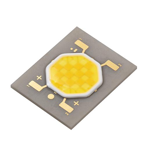
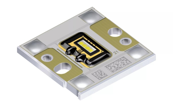
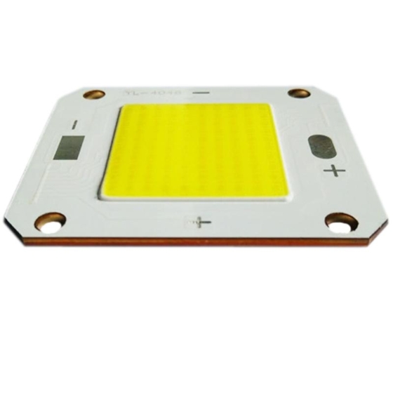
Applications of DBC and DPC Ceramic Substrates in LED Packaging
A Technical Application Guide to Thermal Management, Electrical Insulation, and High-Performance LED Modules
Brand: NMMech | Advanced Ceramic Solutions
1. Application Overview: The Growing Role of Ceramic Substrates in LED Packaging
LED technology has advanced far beyond indicator lights and small display components. Today, high-power LEDs are widely used in industrial lighting, outdoor luminaires, automotive lighting, stage and studio lighting, UV curing systems, horticultural lighting, and specialized optical equipment. As LED output and package density increase, designers must manage heat more effectively while maintaining electrical insulation, mechanical stability, and consistent optical performance.
The LED chip converts electrical energy into light, but not all input energy becomes useful optical output. A portion is released as heat, and excessive junction temperature can reduce luminous output, shift color characteristics, accelerate material aging, and shorten service life. For this reason, the thermal path from the LED die to the heat sink is a central consideration in high-power LED packaging.
Ceramic circuit substrates offer a solution where electrical insulation and thermal performance must be considered together. Direct Bonded Copper (DBC) and Direct Plated Copper (DPC) are two technologies used to create conductive copper patterns on ceramic materials. They serve different design needs and should be selected according to LED power, circuit geometry, thermal requirements, package size, production volume, and reliability targets.
This article explains how DBC and DPC ceramic substrates can be used in LED packaging, where each technology may be suitable, and what product developers should consider when specifying a substrate for a lighting project.
2. Why Thermal Management Matters in LED Packages
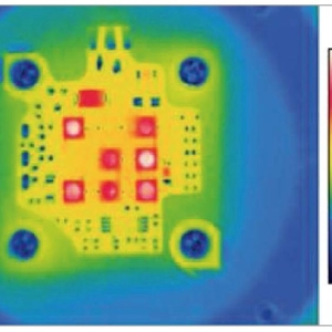
Thermal management is not simply a way to prevent a component from becoming too hot. It directly affects the stability, efficiency, and long-term reliability of an LED system. When heat cannot leave the package efficiently, the LED junction temperature rises. Depending on the LED type and operating conditions, this can contribute to lower light output, wavelength or color shift, faster degradation of encapsulants and other materials, and a greater risk of premature failure.
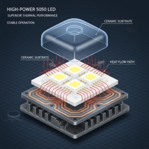
A typical thermal path may include the LED semiconductor die, die-attach material, substrate metallization, ceramic layer, solder or thermal interface material, heat spreader, and heat sink. Each interface adds thermal resistance, so the entire assembly must be designed as a system. A ceramic substrate can contribute to this thermal path, but it does not determine the final junction temperature on its own. Die attachment, copper layout, substrate thickness, heat-sink design, airflow, interface materials, and assembly quality are also important.
Ceramic substrates can provide a combination of electrical insulation and heat transfer. Alumina (Al₂O₃) is widely used because it offers a practical balance of properties and cost. Aluminum nitride (AlN) has higher thermal conductivity than alumina in many commercial grades and may be considered where thermal performance is a priority. The appropriate material depends on the required thermal resistance, electrical insulation, mechanical requirements, manufacturing process, and total cost.
For LED designers, the goal is not to choose the substrate with the highest advertised thermal conductivity in isolation. It is to develop a reliable package with a suitable thermal path, stable electrical behavior, manufacturable circuit patterns, and repeatable production quality.
3. What Is a DBC Ceramic Substrate?
DBC stands for Direct Bonded Copper. In this technology, copper is bonded directly to a ceramic surface through a controlled high-temperature process. Common ceramic materials include alumina and aluminum nitride. Depending on the design, copper may be present on one side or both sides of the ceramic, and the copper can be patterned to form the required circuit.
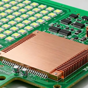
For LED packaging, DBC can be considered when a design needs relatively thick copper, robust conductive paths, and a ceramic insulating layer. The copper can carry current and spread heat laterally, while the ceramic provides electrical isolation and contributes to heat transfer toward the package’s thermal interface. The exact performance depends on the ceramic grade, copper thickness, substrate dimensions, pattern design, and bonding quality.
DBC may be useful in high-power LED modules, demanding lighting assemblies, and packages where current handling and heat spreading are important. It can also be evaluated for LED arrays and power-dense light engines. However, not every LED application needs DBC. For small or fine-pitch packages, the required circuit resolution, package dimensions, and cost targets may make another substrate technology more appropriate.
When assessing DBC, engineers should review copper thickness, minimum circuit features, ceramic material, substrate flatness, copper adhesion, dimensional tolerances, and thermal-cycle requirements. The finished assembly should be evaluated with the actual die attach, solder, heat sink, and operating profile in mind.
4. What Is a DPC Ceramic Substrate?
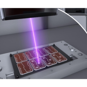
DPC stands for Direct Plated Copper. DPC generally uses metallization and plating processes to form copper layers and circuit patterns on a ceramic substrate. Depending on the supplier’s process and design, DPC can support fine circuit features and precise pattern definition, making it attractive for compact electronic packages and designs that require detailed conductor layouts.
In LED packaging, DPC can be considered for compact LED modules, ceramic LED packages, high-density arrays, and applications where accurate conductor geometry is important. It may support controlled pad layouts, narrow conductor features, and integration of multiple electrical connections within a limited footprint. These characteristics can be useful for miniaturized lighting products and specialized LED assemblies.
DPC is not automatically superior to DBC in every situation. The suitable copper thickness, current capacity, thermal performance, circuit resolution, and manufacturing cost depend on the specific construction and supplier capability. If the design requires high current through thick copper paths, the engineer should confirm whether the proposed DPC stack-up meets the electrical and thermal requirements. If fine patterning and compact layout are key priorities, DPC may be a strong candidate.
A practical DPC specification should include ceramic type and thickness, copper thickness, minimum line width and spacing, pad dimensions, surface finish, overall dimensions, tolerances, and any requirements for solderability or die attachment. Prototype testing can help confirm that the design performs as expected under real operating conditions.
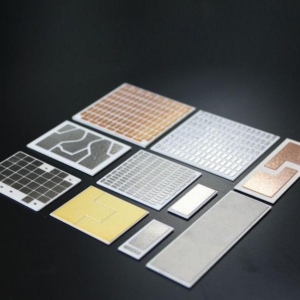
5. DBC vs. DPC for LED Packaging
DBC and DPC both combine ceramic insulation with copper conductors, but their manufacturing approaches and typical design strengths differ. DBC forms a direct copper-to-ceramic bond using a controlled high-temperature process, while DPC generally builds copper metallization through plating-related processes. These differences can influence available copper thickness, achievable pattern detail, process economics, and design flexibility.
DBC is often considered for designs that need relatively thick copper and robust current paths. It can be a suitable option for high-power LED modules where current handling and lateral heat spreading are important. DPC is often considered when fine-line patterning, compact circuits, or more detailed pad geometry is needed. The actual capability range varies by supplier and product configuration, so these are general tendencies rather than universal rules.
Selection should begin with the LED package requirements. Key questions include:
- What is the electrical power per package?
- What current must the copper conductors carry?
- How much heat must be transferred away from the LED die?
- What are the required line width, spacing, and pad geometry?
- What are the operating temperature range and expected service life?
- Is the product intended for a small prototype run or high-volume manufacturing?
A useful comparison should include the complete package, not only the substrate. Thermal resistance across the die attach, substrate, interface material, and heat sink may dominate the result. Likewise, circuit reliability depends on solder quality, bonding interfaces, mechanical stress, and the way the product is assembled. The best solution is the one that meets validated requirements at the required quality and cost.
6. LED Applications Where DBC and DPC May Be Used
6.1 High-Power Industrial and Outdoor Lighting
High-output LED arrays used in industrial facilities, street lighting, floodlights, and area lighting may generate substantial heat. A ceramic substrate can provide electrical isolation and a thermal path while supporting the circuit layout.
DBC may be evaluated for designs requiring robust current paths and relatively thick copper. DPC may be suitable for lighting modules that need more detailed conductor patterns or compact circuit layouts. The choice should be based on power density, thermal design, electrical requirements, and manufacturing constraints.
6.2 Automotive and Transportation Lighting
Headlamps, auxiliary lamps, signal lights, and specialized vehicle lighting may require compact packaging, stable operation, and resistance to environmental stress. Substrate selection should consider LED power level, optical requirements, thermal design, vibration, moisture exposure, and the relevant qualification process.
The ceramic substrate is only one part of a complete automotive-grade assembly. The LED die, attachment materials, connectors, thermal interface, housing, and assembly process all contribute to the final performance and reliability.
6.3 UV LED Systems
UV LEDs are used in curing, printing, inspection, and specialized industrial processes. Many UV LED packages have demanding thermal requirements, and some designs use ceramic substrates to help transfer heat while electrically isolating conductors.
Material selection must also consider the optical system and the temperature limits of surrounding materials. The substrate, die attachment, cooling structure, and operating conditions should be assessed together.
6.4 Horticultural and Specialty Lighting
LED systems used for plant growth, laboratory lighting, and controlled-environment agriculture can contain dense arrays of emitters. Thermal consistency across the array can influence performance and lifetime.
The substrate and circuit pattern should be selected based on power distribution, layout density, cooling design, expected operating hours, and maintenance requirements. A suitable ceramic substrate can support a compact design while contributing to the electrical and thermal management strategy.
6.5 Stage, Studio, and Projection Lighting
High-brightness LED engines may combine multiple chips or color channels in a compact package. Ceramic substrates can support electrical routing and thermal management, but designers must also consider optical alignment, color mixing, package geometry, and serviceability.
These examples are application categories, not a guarantee that every product in the category requires DBC or DPC. The final selection should be based on engineering requirements and verified performance.
 7. Key Design Parameters for LED Ceramic Substrates
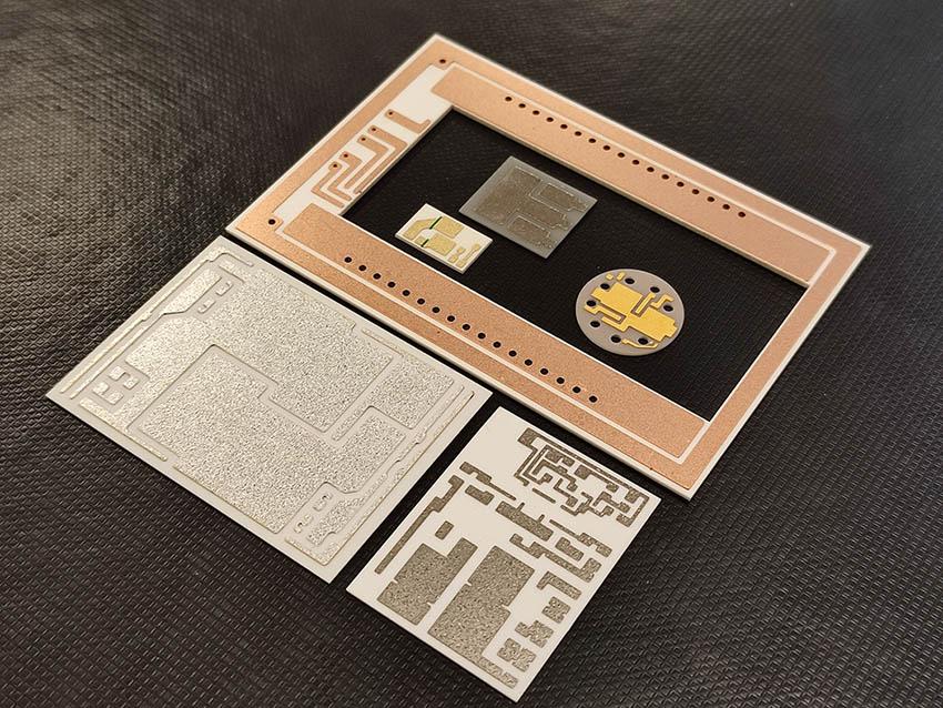 7. Key Design Parameters for LED Ceramic Substrates
Ceramic Material
Alumina is a common choice for many designs because of its balance of electrical, thermal, mechanical, and cost properties. Aluminum nitride may be considered when higher thermal conductivity is required, subject to cost, availability, and design constraints. Material selection should be based on the package’s actual thermal and electrical requirements.
Copper Thickness and Circuit Pattern
Copper thickness affects conductor resistance, current capacity, heat spreading, and patterning limits. Pattern geometry must match the LED’s electrical connections and should account for current density, spacing, solder pads, and manufacturing tolerances.
Thick copper can be useful in some high-current designs, while fine-pitch circuits may favor a different process window. The substrate manufacturer should review the circuit drawing and confirm that the required features can be produced consistently.
Substrate Dimensions and Thickness
Overall size, ceramic thickness, flatness, and dimensional tolerances affect package integration and thermal behavior. The substrate should fit the mechanical envelope and assembly process, including die bonding, soldering, and mounting to the heat sink.
Thermal Design
Define the target thermal resistance or temperature limits for the complete assembly. Consider die attach, substrate, interface materials, heat spreader, heat sink, and cooling conditions. Where possible, validate the design through thermal simulation and measurements on prototypes.
Electrical Insulation and Safety
Determine working voltage, transient conditions, isolation requirements, conductor spacing, and applicable standards. Creepage and clearance requirements depend on the design and operating environment and should be checked at the assembly level.
Reliability and Manufacturing
Consider thermal cycling, power cycling, humidity, vibration, solderability, copper adhesion, and expected lifetime. Review inspection criteria, traceability, documentation, and supplier process controls. For volume projects, consistency between production lots is as important as a successful prototype.
8. From Prototype to Production: A Practical Collaboration Process
A clear specification helps the substrate manufacturer assess feasibility and recommend a suitable process. For an initial inquiry, provide the LED application, estimated power, operating current and voltage, ceramic material preference, substrate dimensions, copper thickness, circuit drawing or Gerber file, and annual quantity estimate.
If the project is still in development, a preliminary drawing and target performance requirements are still useful. The engineering teams can review line width and spacing, pad layout, copper thickness, thermal path, mechanical fit, tolerances, and process limitations. If necessary, alternative material or process options can be discussed before the design is finalized.
Prototype evaluation should use the intended LED die, die-attach material, soldering process, heat sink, and operating conditions wherever possible. Tests may include dimensional inspection, electrical checks, thermal measurements, solderability evaluation, and reliability testing based on the application. Results should be reviewed against agreed acceptance criteria rather than assumptions based only on material data sheets.
After the design is validated, production planning should cover quality controls, lot traceability, packaging, delivery schedule, and change management. A documented process helps reduce risk when moving from engineering samples to repeat orders.
 9. Conclusion: Choosing the Right Ceramic Platform for LED Performance
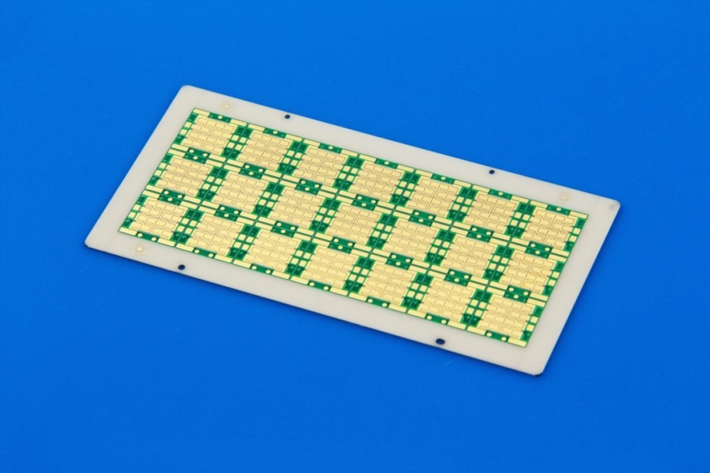 9. Conclusion: Choosing the Right Ceramic Platform for LED Performance
DBC and DPC ceramic substrates can both support LED packages that need electrical insulation, conductive copper patterns, and effective thermal management. DBC may be suitable for robust layouts with relatively thick copper and higher current demands. DPC may be attractive for compact packages and precise circuit patterns. Neither technology is the universal choice; the best option depends on LED power, layout, thermal path, reliability targets, manufacturing requirements, and cost constraints.
A well-designed LED package considers the entire system: semiconductor die, attachment layer, substrate, circuit geometry, thermal interface, heat sink, and assembly process. By defining measurable requirements early and evaluating prototypes under realistic conditions, product teams can make more confident decisions and reduce redesign risk.
NMMech welcomes technical discussions about ceramic substrate requirements for LED packaging. Share your application, drawings, substrate dimensions, ceramic material, copper thickness, circuit features, thermal targets, and estimated order quantity to begin a feasibility review. A well-defined specification helps identify a substrate solution aligned with your performance and production needs.
Contact NMMech to discuss your LED ceramic substrate project and explore a solution tailored to your application.
Suggested SEO keywords: DBC ceramic substrate, DPC ceramic substrate, LED ceramic substrate, high-power LED packaging, LED thermal management, ceramic substrate for LED, LED module substrate.
DBC, DPC, AMB Ceramic Substrates and PCB Industry Resources
Explore industry standards, technical publications, semiconductor manufacturers,
and advanced materials resources related to DBC, DPC, and AMB ceramic substrates,
power electronics, electronic packaging, and PCB manufacturing.
These resources provide useful technical references for engineers, researchers,
procurement professionals, and manufacturers working in power semiconductor
packaging, thermal management, LED technology, and advanced electronic materials.
1. Industry Standards and Associations
1. IPC – Electronics Manufacturing Standards
IPC provides industry standards and technical resources for printed circuit boards,
electronic assemblies, manufacturing processes, quality management, and reliability.
Website:
https://www.ipc.org/
2. JEDEC – Semiconductor Standards
JEDEC develops semiconductor industry standards and technical resources covering
electronic devices, packaging, testing, performance, and reliability.
Website:
https://www.jedec.org/
3. IEC – International Electrotechnical Commission
IEC develops international standards for electrical and electronic technologies,
including areas relevant to electrical insulation, power electronics, and
industrial electronic equipment.
Website:
https://www.iec.ch/
4. IEEE Xplore – Engineering Research
IEEE Xplore provides access to scientific and engineering publications on
semiconductor devices, power electronics, thermal management, and electronic packaging.
Website:
https://ieeexplore.ieee.org/
5. SEMI – Semiconductor Industry Association
SEMI provides industry resources related to semiconductor manufacturing,
materials, equipment, and the global electronics supply chain.
Website:
https://www.semi.org/
2. Ceramic Substrates and Advanced Materials
6. Rogers Corporation – curamik Ceramic Substrates
Rogers provides advanced electronic materials and ceramic substrate solutions
for power electronics, including technologies relevant to DBC and AMB substrates.
Website:
Rogers Ceramic Substrates
7. CoorsTek – Technical Ceramics
CoorsTek develops technical ceramic materials for electronics, semiconductor
manufacturing, industrial equipment, and demanding thermal and electrical applications.
Website:
CoorsTek Products and Applications
8. Ferrotec – Power Electronic Substrates
Ferrotec provides technical and product information related to power electronic
substrates and advanced materials used in electronic systems.
Website:
Ferrotec Power Electronic Substrates
9. ScienceDirect – Scientific Research
ScienceDirect provides access to scientific publications covering ceramic materials,
substrate bonding, thermal conductivity, material properties, and electronic packaging.
Website:
ScienceDirect
10. WellPCB – Ceramic Substrates
WellPCB provides industry information related to ceramic circuit substrates,
ceramic PCB manufacturing, and electronic circuit applications.
Website:
WellPCB Ceramic Substrates
3. Power Semiconductors and Power Electronics
11. Infineon Technologies – Power Modules
Infineon provides semiconductor products and technical information covering
IGBT modules, power conversion, industrial drives, and automotive power electronics.
Website:
Infineon Power Modules
12. Wolfspeed – Silicon Carbide Power Modules
Wolfspeed specializes in silicon carbide technologies and power modules
for high-efficiency power conversion and demanding power electronics applications.
Website:
Wolfspeed SiC Power Modules
13. Mitsubishi Electric – Power Modules
Mitsubishi Electric provides power semiconductor modules for industrial systems,
motor drives, inverters, and automotive power electronics.
Website:
Mitsubishi Electric Power Modules
14. ROHM Semiconductor – SiC Power Devices
ROHM develops silicon carbide power devices for applications such as electric
vehicle power systems, onboard chargers, industrial equipment, and solar inverters.
Website:
ROHM SiC Power Devices
15. onsemi – Silicon Carbide Technology
onsemi provides silicon carbide technologies for electric vehicles,
energy infrastructure, and high-efficiency power conversion systems.
Website:
onsemi Silicon Carbide Technology
4. LED, Electronic Ceramics and PCB Applications
16. Lumileds – LED Technology
Lumileds provides LED technologies for lighting and other optoelectronic
applications, offering useful industry context for high-power LED packaging.
Website:
Lumileds LED Technology
17. CoorsTek – Electronics Applications
CoorsTek develops advanced ceramic materials for electronics, microelectronics,
and other applications requiring specialized electrical, thermal, and mechanical properties.
Website:
CoorsTek Electronics
18. EBest PCBA – Ceramic PCB
EBest PCBA provides information about ceramic printed circuit boards,
manufacturing processes, and specialized electronic applications.
Website:
EBest Ceramic PCB
19. PW Ceramic – DBC, DPC and AMB Comparison
This technical resource discusses differences among Direct Bonded Copper (DBC),
Direct Plated Copper (DPC), and Active Metal Brazed (AMB) ceramic substrate technologies.
Website:
DBC, DPC and AMB Ceramic Substrate Comparison
20. HilPCB – Ceramic PCB
HilPCB provides information about ceramic circuit boards, manufacturing processes,
and ceramic PCB applications in electronic systems.
Website:
HilPCB Ceramic PCB
About NMMech
NMMech focuses on the research, development, and manufacturing of precision
ceramic substrates, including Direct Bonded Copper (DBC) and Direct Plated Copper
(DPC) products. Our solutions serve applications in power electronics, LED packaging,
optoelectronic communications, sensors, and related industries.
We support customized substrate requirements based on project specifications,
including ceramic material selection, substrate dimensions, copper thickness,
circuit patterns, and application conditions.
Visit the NMMech Official Website
External links are provided for informational and technical reference purposes.
Their inclusion does not imply endorsement, certification, partnership,
or formal affiliation with NMMech. Please consult the relevant websites
for current technical information and applicable standards.