 김
 Advanced Power Electronic Substrates: 증권 시세 표시기, AMB and DPC Ceramic Solutions for Next-Generation Electronics
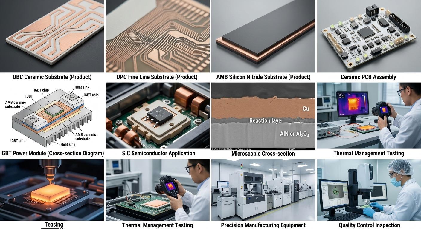
(Explore DBC, 증권 시세 표시기, and DPC ceramic substrates for EV power modules, renewable energy, industrial electronics, and optoelectronic packaging. Discover material selection and custom substrate solutions with NMMech.)
Introduction: The Critical Role of Ceramic Substrates in Power Electronics
As power electronics continue to evolve, manufacturers are under increasing pressure to improve power density, energy efficiency, thermal management, 전기 절연, and long-term reliability. Electric vehicles, renewable energy systems, industrial automation, rail transportation, high-performance power supplies, and advanced semiconductor modules all depend on electronic components that can operate reliably under demanding electrical and thermal conditions.
At the heart of many of these systems is the power electronic substrate. Unlike conventional printed circuit boards designed primarily for low- or moderate-power electronic circuits, ceramic power substrates combine electrical insulation with thermal management and a mechanically stable platform for mounting and interconnecting power semiconductor devices.
Direct Bonded Copper (증권 시세 표시기), Active Metal Brazed (증권 시세 표시기), and Direct Plated Copper (DPC (디씨)) are three important substrate technologies. Each uses a different manufacturing approach and offers a different balance of thermal performance, mechanical properties, circuit precision, and application suitability.
For engineers and procurement teams, choosing the right substrate is not simply a matter of selecting a ceramic material. It requires a system-level assessment of operating temperature, voltage, current, thermal cycling, mechanical stress, circuit geometry, assembly process, and total cost.
NMMech focuses on advanced material solutions, including ceramic substrates and related electronic materials, with an emphasis on application requirements, technical communication, and customized development. This guide introduces the major substrate technologies, explains their characteristics, and outlines the factors that help engineers select an appropriate solution.
1. What Is a Power Electronic Substrate?
A power electronic substrate is an insulating structural component that supports conductive circuit patterns and power semiconductor devices. It is commonly used in power modules containing devices such as insulated-gate bipolar transistors (IGBTs), 실리콘 카바이드 (SiC) MOSFETs, and other semiconductor components designed for power conversion and control.
A typical ceramic power substrate consists of three functional elements:
- Ceramic insulating layer: Provides electrical isolation between conductive regions and the supporting structure while contributing to heat transfer.
- Metal circuit layer: Usually copper, although other metal configurations may be used for specific designs. The patterned metal forms electrical paths and provides a surface for mounting and interconnecting components.
- Optional surface finishes or metallization: Depending on the design, surface treatments may support soldering, wire bonding, corrosion resistance, or subsequent assembly.
The substrate serves several functions simultaneously. It must electrically isolate circuits, transfer heat away from semiconductor devices, maintain adequate mechanical integrity, and withstand stresses caused by temperature changes and differences in thermal expansion.
These requirements are closely connected. A material with excellent thermal conductivity may not automatically provide the best mechanical reliability or the lowest manufacturing cost. Likewise, a substrate that supports fine circuit patterns may not be the most appropriate option for every high-current power module.
Therefore, substrate selection should begin with the electrical, thermal, mechanical, and manufacturing requirements of the final application.
 2. Why Ceramic Substrates Matter in High-Power Electronics
 2.
2.1 Thermal management
Power semiconductor devices generate heat during operation. If this heat is not transferred efficiently to the cooling system, junction temperatures can rise, electrical performance may deteriorate, and component lifetime may be reduced.
A ceramic substrate provides a thermal pathway from the semiconductor assembly toward a baseplate, heat spreader, or cooling structure. The effectiveness of the complete thermal path depends on multiple factors, including ceramic thermal conductivity, layer thickness, interface materials, bonding quality, and the design of the cooling system.
For demanding applications, engineers should evaluate the thermal resistance of the complete assembly rather than relying solely on the thermal conductivity value of the ceramic material.
2.2 전기 절연
High-voltage and high-current power systems require reliable electrical isolation between conductive regions and other parts of the assembly. Ceramic materials can provide the dielectric properties needed for many power electronic designs.
However, insulation performance is influenced by more than the ceramic itself. Substrate thickness, circuit spacing, edge geometry, contamination, humidity, operating temperature, and assembly conditions can all affect electrical reliability.
The final design should therefore be validated against the applicable voltage, creepage, clearance, and environmental requirements.
2.3 Mechanical reliability and thermal cycling
During operation, a power module may experience repeated heating and cooling. Copper and ceramic materials have different coefficients of thermal expansion, so temperature changes can generate stress at their interface.
Over time, excessive stress may contribute to cracking, 갈라짐, fatigue, or other reliability problems. The magnitude of these effects depends on the materials, substrate structure, copper thickness, geometry, joining method, and actual operating conditions.
For applications such as electric vehicle traction inverters, industrial drives, and railway converters, thermal cycling and mechanical loading should be considered early in the substrate selection process.
2.4 Integration and manufacturing compatibility
The substrate must also fit the customer’s assembly process. Die attachment, soldering, wire bonding, 금속, circuit etching, baseplate attachment, and inspection methods can influence the required substrate design.
A technically suitable ceramic material may still be unsuitable if its surface finish, dimensional tolerances, or copper pattern does not match the downstream manufacturing process.
The best solution is one that satisfies both the operating requirements and the practical requirements of production.
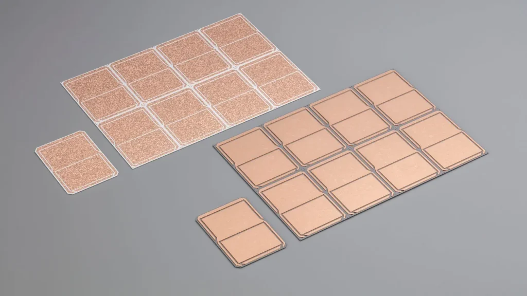
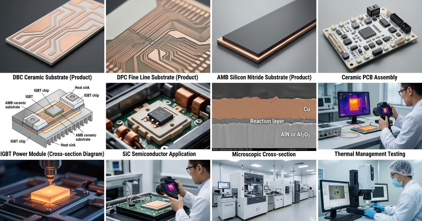
3. Direct Bonded Copper (증권 시세 표시기) 기판
<figure>
<AsyncImage query=”direct bonded copper DBC ceramic substrate alumina copper circuit patterned copper plate close up industrial electronics” aspectRatio=”16:9″ width=”100%” radius=”lg” />
<caption>Suggested image: DBC ceramic substrate with patterned copper circuits.</caption>
</figure>
3.1 What is DBC?
Direct Bonded Copper (증권 시세 표시기) is a ceramic substrate technology in which copper is bonded directly to a ceramic surface through a controlled high-temperature bonding process. Common ceramic options include alumina (알₂O₃) and aluminum nitride (알엔(AlN)), depending on the required thermal and electrical performance.
접착 후, the copper layer can be patterned to create electrical circuits. The resulting structure combines a ceramic insulating layer with conductive copper, allowing the substrate to support power semiconductor devices while transferring heat toward the cooling structure.
DBC is widely used in power electronics where electrical insulation, thermal management, and patterned copper circuits are required.
3.2 Key characteristics of DBC
DBC substrates can offer several useful characteristics:
- Integrated electrical insulation: The ceramic layer separates conductive regions from the supporting structure.
- Effective heat transfer: Thermal performance depends on the ceramic grade, thickness, interfaces, and overall assembly.
- Patterned copper circuits: Copper can be processed into layouts suited to the electrical design.
- Established application experience: DBC is used in a range of industrial and power electronic applications.
- Flexible design options: Ceramic thickness, copper thickness, circuit pattern, substrate dimensions, and selected surface finishes may be specified according to project requirements.
The final performance of a DBC substrate depends on the complete design and manufacturing process. Engineers should review not only the ceramic specification but also copper bonding quality, pattern accuracy, substrate flatness, edge condition, and compatibility with the intended assembly method.
3.3 Common DBC applications
DBC substrates may be considered for:
- Industrial power modules and motor drives
- Switching power supplies and power conversion equipment
- Inverters for selected renewable energy systems
- Automotive power electronics, subject to application-specific requirements
- Home appliance power modules
- Solid-state relays and other power control devices
DBC is often a practical starting point when a project requires ceramic electrical insulation and copper circuit integration with a well-established manufacturing approach.
3.4 When should engineers evaluate DBC?
DBC is worth evaluating when the design requires patterned copper on a ceramic insulating layer and when the combination of thermal performance, mechanical properties, and cost aligns with the application’s requirements.
The choice between alumina-based DBC and aluminum-nitride-based DBC should be based on heat dissipation needs, insulation requirements, mechanical design, operating conditions, and cost targets. Higher thermal conductivity may justify a different ceramic material, but it should be assessed in the context of the complete module.
 4. Active Metal Brazed (증권 시세 표시기) 기판
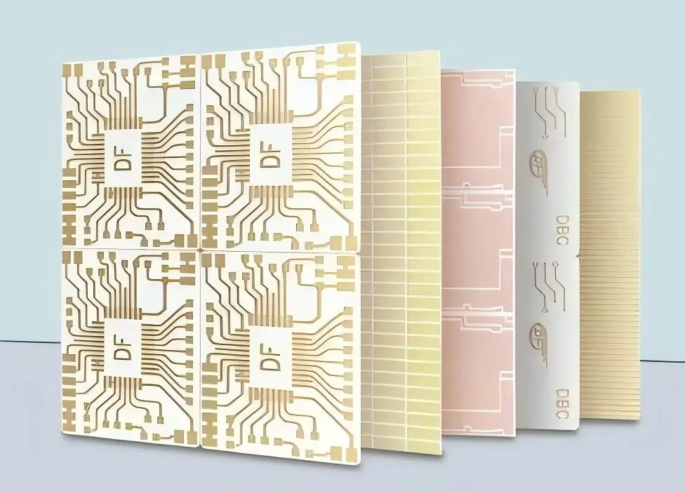 4.
Silicon nitride AMB ceramic substrate thick copper power semiconductor module substrate close
Suggested image: AMB ceramic substrate designed for demanding power electronics.
4.1 What is AMB?
Active Metal Brazed (증권 시세 표시기) is a ceramic substrate technology in which copper is joined to ceramic using an active-metal brazing process. Silicon nitride (Si₃N₄) and aluminum nitride (알엔(AlN)) are important ceramic options for AMB designs.
The active brazing method enables the metal and ceramic to be joined through a specially designed interface. 접착 후, copper can be patterned to create the circuit required by the power module.
AMB is particularly relevant to applications in which mechanical reliability, thermal performance, and resistance to repeated thermal stress are important design considerations.
4.2 Why silicon nitride AMB attracts attention
Silicon nitride ceramic is known for combining useful thermal conductivity with high mechanical strength and fracture toughness compared with many conventional technical ceramics. These properties can make silicon nitride AMB an attractive candidate for power modules exposed to demanding thermal cycling and mechanical loading.
Nevertheless, substrate reliability depends on the entire structure. Ceramic quality, copper thickness, bonding interface, circuit layout, edge geometry, and module assembly all influence the final result.
Silicon nitride AMB should therefore be selected based on application-specific validation rather than the assumption that one material or joining technology is automatically best for every design.
4.3 Key characteristics of AMB
Depending on material selection and design, AMB substrates can provide:
- A robust metal-to-ceramic joining structure
- Good suitability for demanding thermal-cycle environments
- Electrical insulation through the ceramic layer
- Copper circuit patterns for power semiconductor integration
- Design options for high-performance power modules
The balance of properties varies with ceramic type, material thickness, bonding parameters, copper configuration, and downstream assembly conditions.
4.4 Common AMB applications
AMB is frequently considered for demanding power electronic applications such as:
- Electric vehicle traction inverters
- Hybrid vehicle power modules
- Railway traction and auxiliary power converters
- High-power industrial drives
- Power conversion systems with severe thermal cycling
- Selected renewable energy and power transmission equipment
For these applications, the substrate must be evaluated as part of the complete module, including semiconductor die attachment, interconnects, baseplate or cooling structure, and the expected mission profile.
4.5 When should engineers evaluate AMB?
AMB is worth considering when the application places strong emphasis on mechanical robustness, thermal cycling, and long-term reliability. Silicon nitride AMB may be especially relevant where high mechanical performance is required, while aluminum nitride AMB may be considered when thermal conductivity is a major priority.
The decision should account for the specific combination of thermal conductivity, mechanical strength, insulation requirements, copper thickness, module design, and cost. Engineers should compare verified material and assembly data rather than relying on the process name alone.
 5. Direct Plated Copper (DPC (디씨)) 기판
 5.
<figure>
<AsyncImage query=”DPC direct plated copper ceramic substrate fine line precision copper traces white alumina ceramic electronics close up” aspectRatio=”16:9″ width=”100%” radius=”lg” />
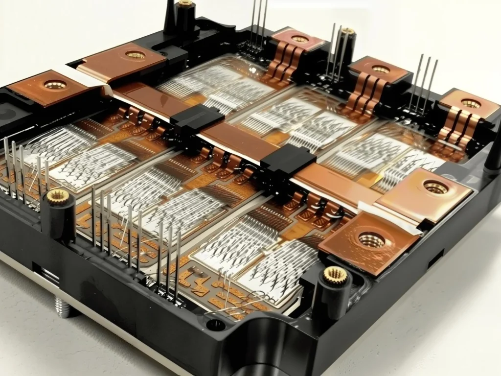
<caption>Suggested image: DPC substrate featuring fine copper circuit patterns.</caption>
</figure>
5.1 What is DPC?
Direct Plated Copper (DPC (디씨)) is a substrate technology that forms copper layers on a ceramic surface through a plating-based process. It can support precise metallization patterns and is often considered for applications that require finer circuit features or specific surface configurations.
Compared with technologies designed primarily around thicker copper layers for power modules, DPC can be particularly useful in selected applications where circuit geometry, pattern definition, and integration with compact electronic components are important.
The appropriate design depends on ceramic selection, copper thickness, circuit spacing, surface finish, and the requirements of the downstream assembly process.
5.2 Key characteristics of DPC
Depending on the design and manufacturing process, DPC substrates may offer:
- Fine circuit pattern capability
- Integration of copper metallization with ceramic insulation
- Design flexibility for compact electronic assemblies
- Compatibility with selected high-power optoelectronic and semiconductor packages
- Options for customized circuit layouts and surface finishes
The attainable line width, spacing, copper thickness, flatness, and dimensional tolerance should be confirmed with the substrate supplier for each design.
5.3 Common DPC applications
DPC substrates may be considered for:
- High-power LED packages
- Laser diode and optoelectronic assemblies
- Optical communication components
- Selected radio-frequency and microwave devices
- Precision electronic packages
- Specialized sensor and semiconductor assemblies
The exact suitability of DPC depends on the power level, heat flux, circuit dimensions, assembly method, and reliability requirements of the end product.
5.4 When should engineers evaluate DPC?
DPC should be evaluated when the design requires precise copper patterning, compact integration, or a particular metallization structure that fits the application’s electrical and thermal demands.
It should not be treated as a universal replacement for DBC or AMB. Instead, engineers should compare the required circuit geometry, current-carrying capacity, ceramic properties, assembly process, and total system cost before choosing the technology.
 6. DBC vs. AMB vs. DPC (디씨): How to Select the Right Substrate
 6.
The three technologies serve overlapping but distinct design needs. A useful selection process begins with the application’s requirements instead of choosing a technology solely by name.
| Selection factor | 증권 시세 표시기 | 증권 시세 표시기 | DPC (디씨) |
|---|---|---|---|
| Typical joining or metallization approach | Direct copper bonding | Active metal brazing | Copper plating |
| Common design focus | Power circuits with ceramic insulation | Demanding power modules and thermal-cycle conditions | Precise circuit patterns and specialized packages |
| Ceramic options | Commonly alumina or AlN | Commonly Si₃N₄ or AlN | Depends on the application and process |
| Circuit geometry | Patterned copper | Patterned copper | Fine patterns may be achievable, subject to design rules |
| Key engineering considerations | Thermal path, copper bonding, flatness, cost | Thermal cycling, mechanical stress, interface reliability | Pattern resolution, metallization thickness, assembly compatibility |
| Typical application examples | Industrial power modules, power supplies | EV traction modules, railway and demanding power systems | LEDs, optoelectronics, precision electronic packages |
This table is a general engineering guide, not a guarantee of performance. Actual specifications vary by supplier, material grade, manufacturing process, geometry, and test method.
A practical decision framework
Step 1: Define the electrical requirements.
Establish working voltage, current, switching behavior, isolation requirements, and circuit layout. These parameters influence ceramic thickness, conductor dimensions, and spacing.
Step 2: Establish the thermal target.
Estimate power loss, heat flux, operating temperature, cooling conditions, and acceptable thermal resistance. Consider the complete thermal path rather than the ceramic layer alone.
Step 3: Assess mechanical and reliability demands.
Review thermal cycling, vibration, shock, humidity, and expected service life. Identify whether the design requires enhanced mechanical robustness or specific qualification testing.
Step 4: Confirm assembly compatibility.
Specify die attachment, soldering, wire bonding, surface finish, baseplate integration, and inspection requirements. Ensure the proposed substrate is compatible with the customer’s manufacturing process.
Step 5: Balance performance and cost.
Compare the substrate’s verified technical performance, manufacturing yield, customization requirements, and expected production volume. The most suitable solution is the one that meets the design requirements reliably and economically.
7. Ceramic Materials: Alumina, 알루미늄 질화물, and Silicon Nitride
 7.
The ceramic material is a major factor in the performance of a power substrate. Three widely discussed options are alumina, 질화알루미늄, and silicon nitride.
Alumina (알₂O₃)
Alumina is a widely used technical ceramic for electronic substrates. It offers electrical insulation, useful mechanical properties, and a well-established manufacturing base. It is often considered for cost-conscious designs and a broad range of industrial electronic applications.
Its thermal conductivity is generally lower than that of aluminum nitride and many silicon nitride grades, so engineers should assess whether the material meets the thermal budget of the intended application.
알루미늄 질화물 (알엔(AlN))
Aluminum nitride is selected when higher thermal conductivity than conventional alumina is needed while maintaining electrical insulation. It can be useful in power modules and other assemblies where efficient heat transfer is a major design priority.
Material grade, thickness, 가공, surface condition, and assembly interfaces influence its actual performance. The thermal conductivity value of the ceramic should not be mistaken for the thermal performance of the entire finished module.
Silicon Nitride (Si₃N₄)
Silicon nitride is valued for its combination of mechanical strength, fracture toughness, and useful thermal properties. It is often evaluated for demanding power module applications, particularly where thermal cycling and mechanical reliability are key considerations.
Silicon nitride substrates may have a different cost profile from alumina-based solutions. Their use should be justified by the requirements and expected operating conditions of the application.
How to compare ceramic materials
When comparing material options, engineers should request consistent, grade-specific data for:
- Thermal conductivity and test conditions
- Dielectric strength and insulation properties
- Flexural strength and fracture-related properties
- Coefficient of thermal expansion
- Ceramic thickness and dimensional tolerances
- Surface condition and flatness
- Compatibility with bonding, plating, and assembly processes
Material selection should be based on verified specifications and application testing, not on a single property in isolation.
8. Major Application Areas for Ceramic Power Substrates
<figure>
<AsyncImage query=”electric vehicle traction inverter power electronics module opened industrial engineering photography” aspectRatio=”16:9″ width=”100%” radius=”lg” />
<caption>Suggested image: Power electronic module used in electric mobility.</caption>
</figure>
8.1 Electric vehicles and hybrid vehicles
Electric vehicles rely on power electronics to convert and control energy between the battery, traction motor, onboard charger, and other electrical systems. Traction inverters and DC-DC converters may operate under substantial electrical and thermal loads.
Ceramic substrates can help integrate power semiconductor devices while providing electrical insulation and a pathway for heat transfer. The appropriate technology depends on voltage class, current, switching losses, cooling architecture, vibration, thermal cycling, and service-life targets.
For high-demand traction applications, DBC and AMB are both worth evaluating, with the final choice based on the complete module design and validated reliability requirements.
8.2 Renewable energy and energy storage
Solar inverters, wind power converters, and energy storage systems use power semiconductor modules to manage the conversion and flow of electrical energy. These systems may experience changing loads, environmental temperature variations, and long operating periods.
Ceramic substrates can support the electrical and thermal requirements of power conversion assemblies. Selection should consider continuous and peak power, cooling design, environmental conditions, electrical isolation, and the expected operating profile.
8.3 Industrial automation and motor drives
Variable-frequency drives, servo systems, welding equipment, industrial power supplies, and automation systems depend on reliable power conversion. In these environments, substrate selection can affect thermal management, module design, and long-term system reliability.
DBC may be suitable for many established industrial power module designs, while AMB can be evaluated for applications with more demanding thermal-cycle or mechanical requirements.
8.4 Rail transportation and high-power converters
Railway traction systems and auxiliary converters can expose power modules to demanding vibration, temperature changes, and long service cycles. Substrate reliability must be considered together with the module structure, cooling system, assembly process, and maintenance requirements.
증권 시세 표시기, including silicon nitride-based solutions, may be worth evaluating for designs where mechanical robustness and thermal cycling are central considerations.
8.5 LED and optoelectronic packaging
High-power LEDs, laser devices, and selected optical communication components require effective heat management within compact packages. DPC and other suitable ceramic metallization technologies can be considered where precise circuit geometry and package integration are important.
The design should account for heat flux, mounting conditions, electrical layout, optical alignment where applicable, and the requirements of the final package.
8.6 Data infrastructure and specialized electronics
High-performance computing, communication infrastructure, sensing, and other specialized electronics can create demanding requirements for thermal management and packaging. Ceramic substrate technologies may be appropriate in selected assemblies where electrical insulation, heat transfer, and material stability are needed.
The specific substrate technology should be chosen according to the actual device architecture and operating environment rather than assuming that one substrate type is suitable for every data center or communication application.
9. Quality Control: From Material Selection to Finished Substrate
The quality of a ceramic power substrate is determined by more than the nominal material specification. Process control and inspection are essential to ensure that the finished component meets the intended design requirements.
Important quality considerations include:
Raw material consistency. Ceramic composition, thickness, surface condition, and material properties should be controlled against the applicable specification.
Bonding or metallization integrity. For DBC and AMB, the metal-to-ceramic interface is critical. For DPC, plating quality and metallization consistency are important. Inspection and test methods should be selected according to the process and application.
Circuit pattern accuracy. Copper geometry, line width, spacing, edge condition, and registration can influence electrical performance and assembly compatibility.
Dimensional stability and flatness. Substrate dimensions, warpage, and flatness may affect mounting, soldering, and the reliability of the final module.
Surface finish and solderability. Where required, the surface finish should be compatible with the customer’s die attachment, soldering, wire bonding, or other joining process.
Traceability and documentation. Material identification, inspection records, agreed acceptance criteria, and batch traceability can support quality management and customer qualification.
Testing requirements should be defined by the application. Depending on the design, these may include dimensional inspection, visual inspection, bonding or peel-strength assessment, solderability evaluation, electrical testing, thermal cycling, or other qualification tests. Acceptance limits and methods should be agreed upon before production.
10. Customization and Engineering Collaboration
A standard catalog specification is not always sufficient for a specialized power module. Customers may require customized substrate dimensions, copper thickness, circuit patterns, ceramic thickness, surface finishes, or other design parameters.
An effective customization process begins with clear technical communication. To evaluate a project, engineers and procurement teams should prepare the following information where available:
- Application and end-product description
- Substrate technology under consideration: 증권 시세 표시기, 증권 시세 표시기, DPC (디씨), or an alternative
- Ceramic material and thickness
- Copper thickness and circuit drawings
- Overall dimensions, tolerances, and flatness requirements
- Operating voltage, current, and temperature range
- Heat dissipation and cooling conditions
- Assembly method and surface finish requirements
- Expected annual demand and prototype quantity
- Required inspection, qualification, and documentation
If some parameters have not yet been finalized, an initial review can help identify the information needed to proceed. Final design feasibility, tolerances, performance, and lead time must be confirmed against the actual drawing, material availability, manufacturing process, and agreed validation requirements.
11. From Prototype Evaluation to Production
A structured development process can reduce the risk of costly changes after a design enters production.
Stage 1: Requirement review. Confirm the application, operating conditions, drawings, and key performance criteria.
Stage 2: Technical feasibility assessment. Review the ceramic material, metallization method, circuit geometry, dimensions, and manufacturing constraints.
Stage 3: Prototype or sample evaluation. Verify fit, assembly compatibility, electrical and thermal behavior, and any agreed inspection criteria.
Stage 4: Design refinement. Use evaluation results to adjust circuit geometry, material selection, thickness, surface finish, or other parameters where necessary.
Stage 5: Production readiness. Confirm the approved specification, quality requirements, packaging, documentation, and forecast demand before production planning.
Stage 6: Ongoing quality review. Monitor relevant quality data and communicate changes that may affect the approved design or manufacturing process.
The exact sequence depends on project complexity, customer qualification requirements, and the selected substrate technology.
12. Why Work with NMMech?
NMMech operates in the advanced materials and electronic materials field, with a focus on ceramic substrates, copper-clad materials, filtration materials, and related technical solutions. For customers developing power electronic products, the value of a supplier relationship extends beyond the delivery of a physical component.
A productive technical partnership should support clear specification review, communication between engineering and procurement teams, realistic evaluation of material options, and alignment between the substrate design and the final application.
For customized projects, NMMech can work with customers to review drawings and application requirements, clarify critical parameters, and assess suitable material and substrate options. Feasibility, product configuration, manufacturing schedule, testing, and commercial terms should be confirmed individually for each project.
Whether you are developing a new power module, optimizing an existing design, or evaluating alternative ceramic substrate technologies, early technical discussion can help identify the most relevant questions before prototype and production decisions are finalized.
Conclusion: Selecting a Substrate That Fits the Complete System
증권 시세 표시기, 증권 시세 표시기, and DPC ceramic substrates serve important but different roles in modern electronics. DBC provides an established approach for patterned copper on ceramic insulation. AMB is an important option for demanding power modules where the metal-ceramic interface, mechanical properties, and thermal-cycle performance require careful evaluation. DPC can support selected designs that call for precise copper metallization and compact electronic integration.
No single substrate technology is the best choice for every application. The right decision depends on thermal performance, 전기 절연, mechanical stress, circuit geometry, manufacturing compatibility, reliability targets, and total cost.
By evaluating these factors together and validating the proposed design under relevant operating conditions, engineers can select a ceramic substrate that supports the performance and reliability goals of the finished electronic system.
Discuss Your Ceramic Substrate Project with NMMech
Are you sourcing DBC, 증권 시세 표시기, or DPC ceramic substrates for power modules, electric mobility, renewable energy, industrial electronics, or optoelectronic packaging?
Contact NMMech to discuss your application, technical drawings, material requirements, and customization needs.
To help us assess your project, please share your substrate drawing, ceramic material and thickness, copper specifications, operating conditions, expected quantity, and any special testing or documentation requirements.
NMMech — Advanced Materials and Customized Electronic Substrate Solutions.
Technical Resources for Ceramic Substrates and Power Electronics
Explore selected international standards organizations, scientific
research institutions, and academic resources covering ceramic
substrates, electronic packaging, thermal management, PCB technology,
and power electronics reliability.
1. International Standards and Technical Organizations
International Electrotechnical Commission (IEC)
International electrotechnical standards and technical information
relevant to electrical equipment, electronic components, and safety.
Institute of Electrical and Electronics Engineers (IEEE)
A global professional organization supporting research and knowledge
exchange in electrical engineering, electronics, and semiconductor
technologies.
SEMI
Industry information and technical initiatives related to
semiconductor manufacturing, electronics, and advanced technologies.
2. Scientific Research and Academic Publications
IEEE Xplore Digital Library
Research papers and technical publications on power electronics,
semiconductor devices, thermal management, and electronic systems.
ScienceDirect
A scientific literature platform covering materials science,
ceramics, electronics, engineering, and reliability research.
SpringerLink
Academic books and research articles covering advanced materials,
ceramic engineering, electronic packaging, and applied physics.
Google Scholar
A search resource for scholarly literature, including studies on
DBC substrates, DPC metallization, AMB technology, and ceramic materials.
Materials Journal
Scientific articles on material properties, ceramics, interfaces,
manufacturing processes, and material characterization.
3. Government and National Research Institutions
National Institute of Standards and Technology (NIST)
Research and measurement resources for materials characterization,
semiconductor technologies, and engineering reliability.
NIST Thermal Property Measurements
Research on thermal property measurements relevant to semiconductor
materials, 파워 일렉트로닉스, and thermal simulation.
NASA Electronic Packaging Project
Technical information on electronic packaging assessment, validation,
reliability, and testing for demanding applications.
NASA
Engineering and scientific resources related to high-reliability
electronic systems and advanced technology applications.
4. European Research Institutes and Technology Programs
Fraunhofer Institute for Ceramic Technologies and Systems (IKTS)
Research on technical ceramics, ceramic-based power electronics,
materials processing, and electronic systems.
Fraunhofer IKTS: Ceramic DCB Substrates in Power Electronics Research
A research project exploring functionalization of ceramic DCB
substrates and condition monitoring in power electronic modules.
Fraunhofer Institute for Reliability and Microintegration (IZM)
Research in electronic packaging, system integration, interconnection
technologies, and reliability engineering.
Fraunhofer Institute for Integrated Systems and Device Technology (IISB)
Research on semiconductor materials, 파워 일렉트로닉스, device
characterization, and advanced electronic technologies.
5. Technical Papers on DBC Ceramic Substrates
Characterization of Materials and Their Interfaces in a Direct Bonded Copper Substrate
A research article examining copper, ceramic, and interface behavior
in DBC substrates for power electronics applications.
Development of a Ceramic-Based Composite for Direct Bonded Copper Substrate
Research into ceramic composite design and the thermal and structural
properties relevant to DBC substrate applications.
Application of Direct Bonded Copper Substrates for Prototyping of Power Electronic Modules
A technical paper discussing DBC substrate processing approaches
and their application in power electronic module prototyping.
Emerging Trends and Challenges in Thermal Management of Power Electronic Converters
A technical review of thermal management methods and reliability
challenges in power electronic converters.
About NMMech
NMMech focuses on the research, development, and manufacturing of
precision ceramic substrates, including Direct Bonded Copper (증권 시세 표시기)
and Direct Plated Copper (DPC (디씨)) technologies. Our technical focus
includes ceramic materials, copper-to-ceramic interfaces, circuit
pattern requirements, thermal management, and electronic packaging
applications. We support customized substrate development according
to project specifications and application requirements.
Disclaimer: The external resources listed on this page
are provided for educational and technical reference purposes only.
Their inclusion does not imply endorsement, certification, sponsorship,
or any business relationship with NMMech. Availability and access
conditions are determined by the respective website owners.