
![]()
SiC Power Device Fabrication Process Flow
 1. Substrate Preparation
Core Objective: Obtain high-purity, low-defect SiC single-crystal substrates.
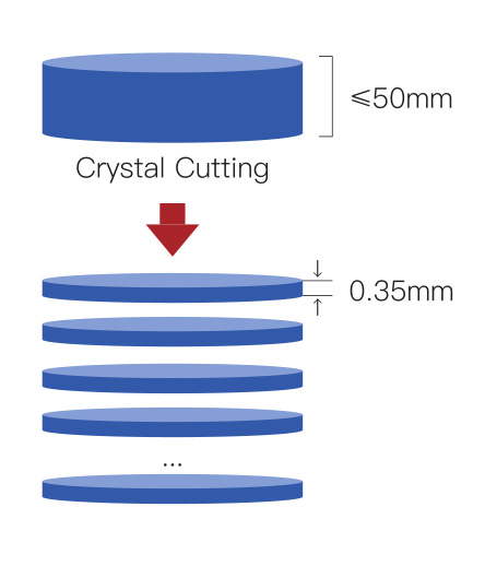
Crystal Growth: SiC powder is sublimated and deposited on a seed crystal via the Physical Vapor Transport (PVT) method at >2000°C, forming a SiC ingot.
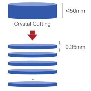
Wafer Processing:
Cutting: Diamond wire saws slice the ingot into wafers (thickness ≤1mm) with edge crack reduction using laser-assisted techniques34.
Polishing: Chemical Mechanical Polishing (CMP) achieves surface roughness <0.5nm.
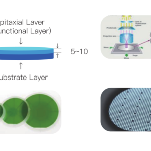
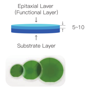
2. Epitaxial Growth
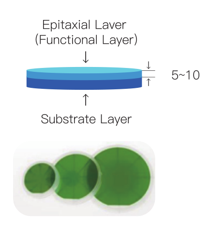
Core Objective: Deposit high-quality SiC epitaxial layers (e.g., N-type drift layers).
Chemical Vapor Deposition (CVD):
Reactants: SiH₄ and C₃H₈ at 1500–1700°C, with in-situ doping (N or Al) for uniform carrier concentration.
Defect Control: Photoluminescence (PL) or X-ray diffraction (XRD) detects dislocation density (<1×10³ cm⁻²).
3. Device Fabrication
Core Objective: Form functional structures (e.g., MOSFET gates, PN junctions).
Oxide Layer Formation:
Dry thermal oxidation (1200–1300°C) or Atomic Layer Deposition (ALD) creates SiO₂/Al₂O₃ gate dielectric layers (interface traps <1×10¹¹ cm⁻²·eV⁻¹).
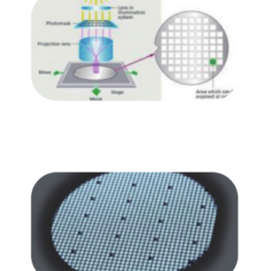
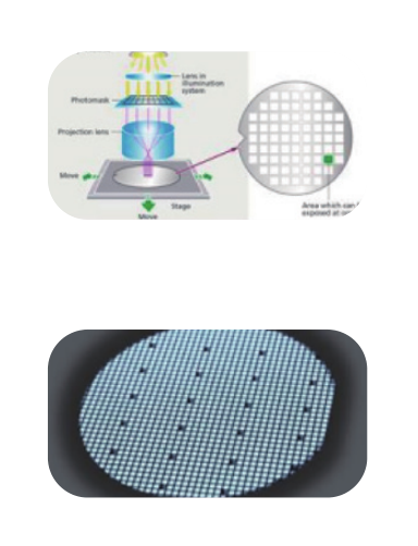
Lithography & Ion Implantation:
Photolithography: UV exposure defines patterns with linewidth ≤0.5μm, adapted for SiC’s hardness using specialized equipment.
Ion Implantation: Al (P-type) or N (N-type) ions are implanted and activated via high-temperature annealing (>1600°C).
Metallization & Etching:
Electrode Deposition: E-beam evaporation of Ti/Al/Ni layers (200–500nm) for source, drain, and gate contacts.
Mesa Etching: Reactive Ion Etching (RIE) isolates devices with etch depths of 3–5μm.
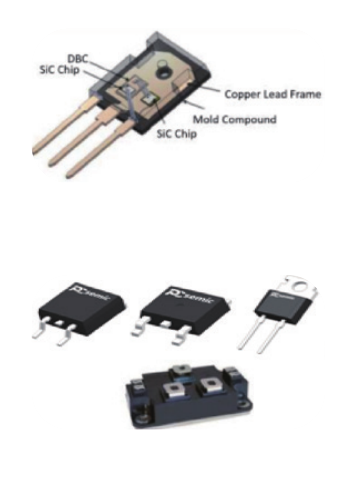
4. Packaging & Testing
Core Objective: Ensure reliability and performance under high-voltage/high-temperature conditions.
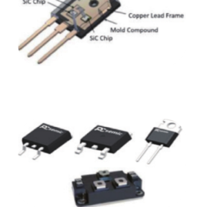
Die Attach:
Silver sintering bonds chips to substrates at 250°C and 20MPa (shear strength >30MPa).
Module Assembly:
Wire Bonding: Au or Al wires connect electrodes.
Encapsulation: High-temperature-resistant materials (e.g., silicone gel) protect against thermal stress.
Electrical Testing:
Static Parameters: Breakdown voltage (Vbr ≥1700V), on-resistance (Rds(on) <50mΩ).
Dynamic Parameters: Double-pulse testing evaluates switching losses (Eoss <10μJ).
Key Process Innovations
Substrate Defect Mitigation: Laser-assisted cutting reduces edge chipping.
Epitaxial Uniformity: In-situ doping optimizes carrier concentration gradients.
Advanced Packaging: Nano-silver paste replaces solder for 250°C operation.
This process integrates the latest advancements from industry and academia, tailored for high-voltage EV and renewable energy applications.

✅Contact us:
website: www.nmmech.com
電子メール: jack@nmmech.com
More industry information:
🌐 1. Advanced Materials / Precision Ceramics
External Link: https://www.azom.com
Description :
Learn more about the latest trends in advanced ceramics and precision materials from AZoM, a global materials science hub that provides insights into material innovations, applications, and manufacturing technologies.
🚀 2. Aerospace Industry
External Link: https://www.nasa.gov
Description:
The aerospace industry relies heavily on high-performance ceramics. Visit NASA to explore how ceramic materials are used in propulsion systems, thermal protection, and structural components in space exploration.
⚙️ 3. Electronics Industry
External Link: https://www.ieee.org
Description:
The electronics and semiconductor sectors depend on materials with high dielectric strength and insulation performance. IEEE is a trusted global organization that drives innovation in electrical and electronic engineering.
💡 4. Semiconductor Industry
External Link: https://www.semiconductors.org
Description:
Discover how advanced ceramics contribute to semiconductor manufacturing — from wafer handling to plasma etching — at the Semiconductor Industry Association (SIA).
🚗 5. Automotive Industry
External Link: https://www.sae.org
Description:
The automotive industry increasingly adopts advanced ceramic components for fuel systems, sensors, and EV batteries. Visit SAE International for standards and innovations driving automotive engineering forward.
🏥 6. Medical & Healthcare
External Link: https://www.fda.gov/medical-devices
Description:
Advanced ceramics play a vital role in medical implants and devices due to their bio-compatibility and wear resistance. The U.S. FDA Medical Devices Center provides regulatory and research information in this field.
⚡ 7. New Energy / Renewable Energy
External Link: https://www.energy.gov
Description:
In the renewable energy sector, ceramics are used for high-temperature fuel cells and power electronics. Visit the U.S. Department of Energy (DOE) for innovations and materials research in sustainable energy technologies.
")


