 GIM
 DBC Ceramic Substrate Manufacturing Process: From Raw Materials to High-Reliability Power Electronics
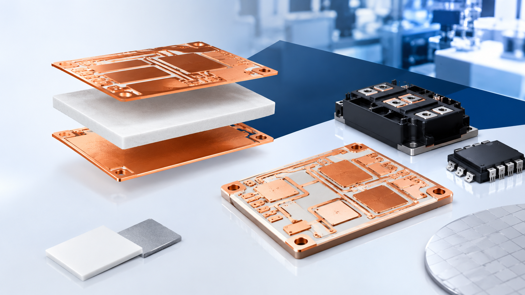
A Technical Guide to Direct Bonded Copper Technology, Circuit Fabrication, Quality Control, and Industrial Applications
Brand: NMMech | Advanced Ceramic Solutions
1. Introduction: Why DBC Manufacturing Quality Matters
As power electronics continue to develop toward higher power density, improved efficiency, and more compact designs, ceramic circuit substrates have become important components in many demanding electronic systems. Rame a legame diretto (DBC) ceramic substrates are widely considered for applications that require electrical insulation, effective heat transfer, and reliable copper conductors in the same structure.
DBC substrates are used in power semiconductor modules, including IGBT and SiC power modules, as well as electric vehicle inverters, industrial motor drives, renewable energy converters, and other power conversion systems. In these applications, the substrate is more than a circuit carrier. It helps provide electrical isolation, transfers heat away from power devices, and supports conductive patterns that connect components within the module.
The performance of a finished DBC substrate depends on more than the nominal properties of copper or ceramic. Material consistency, surface preparation, copper-to-ceramic bonding, circuit patterning, dimensional accuracy, cleanliness, and inspection all influence the final result. A defect introduced during an early manufacturing stage may affect later processing or reduce reliability in service.
Understanding the DBC manufacturing process helps engineers evaluate substrate specifications, compare manufacturing options, and communicate more effectively with suppliers. This article introduces the major production stages, explains the purpose of each step, and outlines the quality considerations that matter when developing DBC substrates for demanding applications.
2. What Is a DBC Ceramic Substrate?
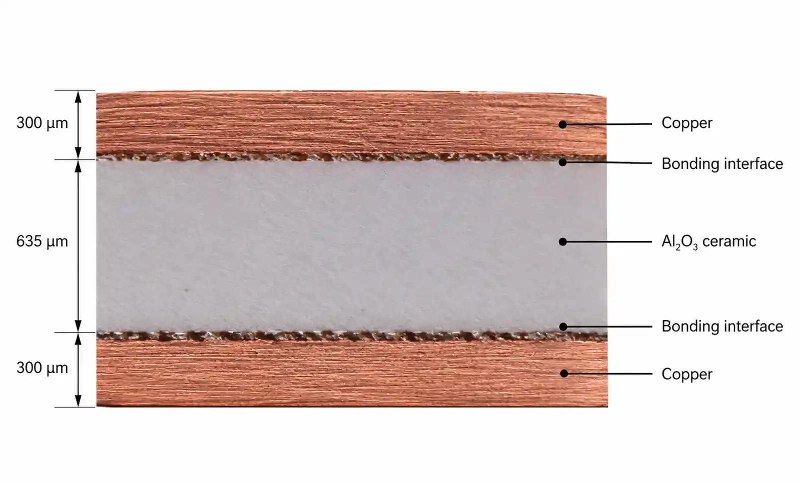
DBC stands for Direct Bonded Copper. It is a ceramic substrate technology in which copper is directly bonded to a ceramic base through a controlled high-temperature process. Common ceramic materials include aluminum oxide (Al₂O₃), also known as alumina, and aluminum nitride (Aln). Depending on the design, copper may be bonded to one side or both sides of the ceramic.
The copper layer serves as an electrical conductor and can also spread heat across the substrate surface. The ceramic layer provides electrical insulation and contributes to the thermal path from the semiconductor device toward the cooling structure. Together, these materials form a platform for fabricating circuit patterns used in power electronic assemblies.
DBC is particularly relevant where engineers need a combination of insulation, heat transfer, and relatively robust copper conductors. The appropriate construction depends on operating voltage, current, thermal resistance targets, mechanical constraints, and reliability requirements. Copper thickness, ceramic thickness, substrate dimensions, and circuit geometry must therefore be selected as part of the complete module design.
DBC is different from a conventional organic printed circuit board made with materials such as FR-4. It is also different from DPC (Direct Plated Copper) and AMB (Brasatura attiva dei metalli), which use different metallization or bonding approaches. The choice among these technologies should be based on the application requirements rather than on a single material property.
 3. Overview of the DBC Manufacturing Workflow
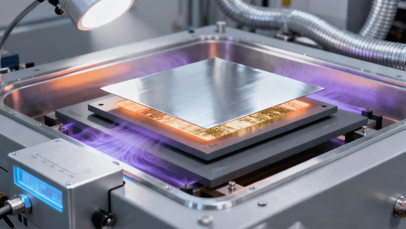 3.
Although manufacturing details vary among suppliers, a typical DBC production workflow includes the following stages:
- Ceramic material selection and incoming inspection.
- Copper foil selection and preparation.
- Ceramic and copper surface preparation.
- Direct copper-to-ceramic bonding under controlled process conditions.
- Cooling and initial bonding inspection.
- Circuit design transfer and photoresist patterning.
- Copper etching and removal of unwanted material.
- Photoresist stripping and cleaning.
- Dimensional, visual, and electrical inspection.
- Additional finishing, testing, packaging, and shipment as required.
These stages are closely connected. The quality of the incoming materials affects bonding, while the bonding result influences circuit fabrication and later reliability. A stable manufacturing process therefore requires controls at each stage rather than relying only on final inspection.
4. Step One: Ceramic Material Selection and Preparation
The ceramic base is a fundamental part of a DBC substrate. Its material properties affect electrical insulation, thermal performance, mechanical behavior, and the suitability of the finished substrate for the intended operating environment.
Alumina and Aluminum Nitride
Alumina is commonly selected because it offers a practical balance of electrical insulation, mechanical properties, availability, and cost. Aluminum nitride is often considered when higher thermal conductivity is required, although material selection must also account for cost, design constraints, and manufacturing compatibility.
Neither material is automatically the best choice for every project. Engineers should evaluate thermal resistance, working voltage, substrate dimensions, thermal cycling, mechanical stress, and the complete cooling arrangement before deciding.
Incoming Inspection
Before production, ceramic plates may be inspected for dimensions, thickness, flatness, surface condition, visible defects, and other specification-dependent characteristics. The inspection criteria should reflect the intended product and agreed quality requirements.
Surface contamination, cracks, chips, or excessive dimensional variation can create processing difficulties or affect the finished substrate. Appropriate handling and storage are therefore important, particularly for thin or fragile ceramic components.
Surface Preparation
The ceramic surface must be suitable for the bonding process. Depending on the manufacturing route, preparation may include cleaning and other controlled treatments designed to reduce contamination and support consistent bonding. Exact methods are process-specific and should be established by the manufacturer.
The purpose of this stage is to provide a consistent starting surface for copper bonding and reduce the risk of defects associated with uncontrolled surface conditions.
 5. Step Two: Copper Foil Selection and Preparation
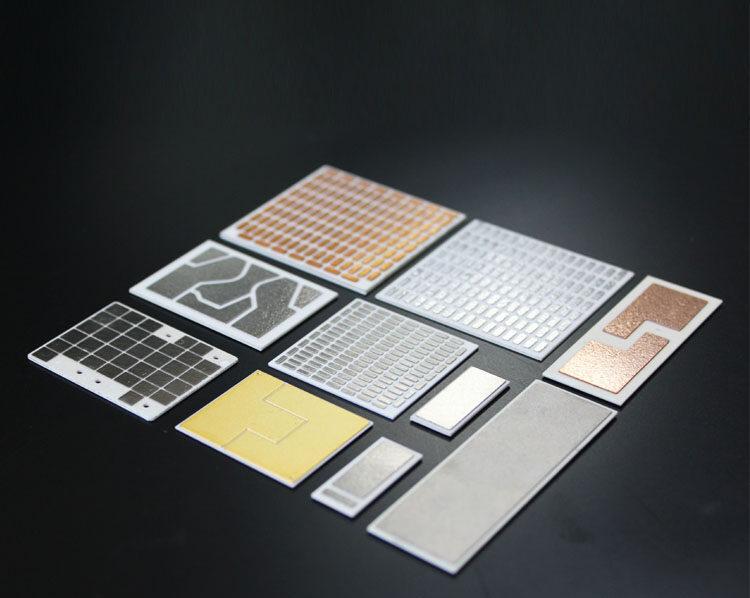 5.
Copper forms the conductive layer of a DBC substrate. Its thickness, surface quality, and consistency affect current-carrying capability, resistance, heat spreading, circuit geometry, and manufacturing yield.
Choosing the Copper Thickness
The required copper thickness depends on current, conductor width, circuit layout, thermal design, and mechanical requirements. Thicker copper may be useful for some high-current applications, while thinner copper may be appropriate for other circuit designs or package constraints.
The design must balance electrical and thermal performance with the minimum achievable circuit features, substrate dimensions, etching capability, and cost. Copper thickness should be defined together with line width, spacing, pad geometry, and dimensional tolerances.
Copper Quality and Surface Condition
Incoming copper should be checked against the relevant material specifications. Depending on the product, checks may cover thickness, surface appearance, contamination, and material traceability. Surface preparation is important because uncontrolled contamination or surface variation can interfere with bonding or subsequent processing.
Good material management helps maintain consistency between production lots and supports root-cause analysis if a quality issue occurs.
6. Step Three: Direct Copper-to-Ceramic Bonding
The defining stage of DBC manufacturing is the direct bonding of copper to ceramic. In a typical process, copper and a suitable ceramic material are brought together under carefully controlled high-temperature conditions. For commonly used DBC systems, the bonding mechanism involves copper and oxygen-related surface chemistry that enables the copper to bond to the ceramic.
The process requires a suitable combination of material composition, surface condition, temperature profile, atmosphere, time, and cooling conditions. The precise recipe depends on the ceramic type, copper specification, equipment, and manufacturer’s validated process window.
Why Process Control Is Important
If bonding conditions are not properly controlled, the interface may develop defects, local non-bonded regions, or inconsistent adhesion. Excessive thermal stress may also contribute to warpage or damage, depending on the materials and substrate geometry.
Manufacturers therefore need to control the process consistently and verify that the resulting interface meets the specified requirements. Temperature uniformity, equipment condition, material preparation, and loading arrangements may all affect the result.
Cooling and Initial Inspection
After bonding, the substrate is cooled according to the established process. Initial inspection may include visual checks, dimensional measurements, flatness evaluation, and other tests selected for the product.
The bonded copper should remain sufficiently attached to the ceramic through later processing and intended service conditions. Bond integrity is especially important for power modules exposed to repeated heating and cooling during operation.
 7. Step Four: Circuit Pattern Design and Transfer
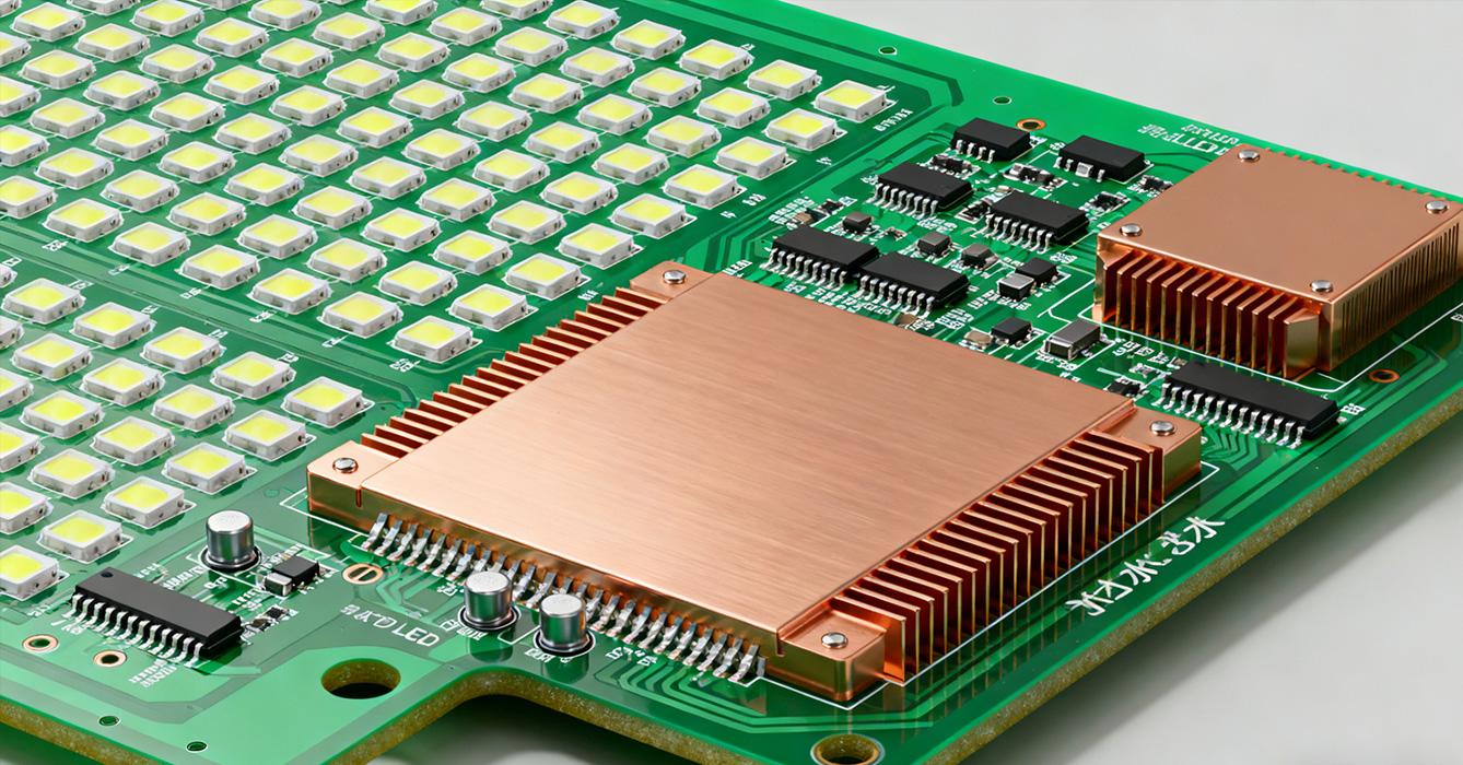 7.
After the copper has been bonded, the substrate is processed to create the required circuit layout. The copper surface is patterned so that the finished substrate contains the conductive areas, pads, and isolation gaps needed by the electronic design.
Circuit Design Preparation
The circuit layout should be reviewed before manufacturing. Important items include conductor width, spacing, pad dimensions, current paths, isolation distances, edge clearances, and alignment with the module’s assembly features.
For power electronics, the layout can influence current distribution, parasitic electrical characteristics, heat spreading, and assembly reliability. The design must also comply with the applicable electrical and mechanical requirements.
Photoresist Patterning
A common circuit fabrication route uses a photosensitive resist and a pattern-transfer process. The intended circuit image is transferred to the copper surface, allowing selected areas to be protected during etching while unwanted copper is removed.
The accuracy of this step affects line geometry and the definition of isolation gaps. Pattern alignment, resist quality, surface cleanliness, and process stability are important considerations.
The precise patterning method may vary by manufacturer and product specification. Some designs may require different process arrangements according to circuit complexity, copper thickness, and dimensional requirements.
 8. Step Five: Copper Etching and Cleaning
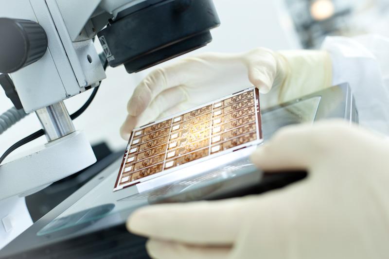 8.
Etching removes the unwanted copper and leaves the required circuit pattern. This step converts the continuous copper layer into electrically separated conductors and functional pads.
Etching Control
Etching conditions must be controlled to achieve the required circuit dimensions without excessive undercutting, incomplete copper removal, or damage to the desired features. Copper thickness and pattern geometry affect the achievable line width and spacing, so the design should be reviewed against the manufacturer’s actual process capability.
Poor etching control may cause open circuits, short circuits, narrow conductors, irregular edges, or dimensional variation. Such defects can affect electrical performance or prevent the substrate from meeting the drawing requirements.
Photoresist Removal and Final Cleaning
After etching, the remaining resist is removed and the substrate is cleaned to eliminate process residues. Cleanliness is important for later assembly operations, including soldering, die attachment, and other connection processes.
The finished copper pattern should be checked for unwanted residue, surface contamination, damaged features, and other visible abnormalities. Where required, additional surface finishing may be specified according to the assembly process and product requirements.
9. Step Six: Dimensional Inspection and Quality Control
Quality control should be integrated throughout the manufacturing workflow. Final inspection is important, but it cannot replace appropriate controls over materials, bonding, and circuit fabrication.
Visual Inspection
Visual inspection can identify visible defects such as scratches, chips, contamination, abnormal discoloration, copper damage, and obvious pattern defects. Inspection methods and acceptance criteria should be defined in the product specification.
Dimensional Inspection
Dimensional checks may include overall length and width, ceramic and copper thickness, flatness, warpage, pattern dimensions, and feature locations. The required measurement method depends on the tolerance and geometry being inspected.
Accurate dimensions help ensure that the substrate fits the intended module, aligns with other components, and can be assembled consistently.
Bond Integrity and Copper Adhesion
The copper-to-ceramic interface is critical to DBC performance. Appropriate tests may be used to assess bond integrity or copper adhesion according to the applicable product specification and test method. Acceptance values should be agreed upon between the customer and supplier rather than assumed to be universal.
Electrical and Functional Checks
Depending on the application, inspection may include circuit continuity, isolation between conductive regions, or other electrical checks. High-voltage power modules may require additional verification at the assembly level, according to the design and relevant standards.
Traceability and Documentation
For demanding industrial applications, traceability helps connect raw materials, manufacturing conditions, inspection records, and finished products. Documentation may include material records, inspection reports, process records, and certificates agreed upon with the customer.
A clear quality plan makes it easier to identify deviations, investigate root causes, and maintain consistency across production lots.
10. Reliability Considerations for DBC Substrates
DBC substrates used in power electronics may experience repeated thermal cycling, power cycling, mechanical stress, and environmental exposure. These conditions can place stress on the ceramic, copper, bonded interface, solder joints, and surrounding assembly.
Reliability depends on the entire module rather than on the substrate alone. Copper thickness, ceramic material, substrate dimensions, circuit layout, die attachment, baseplate design, soldering process, and cooling conditions all influence the stress distribution and service performance.
For applications such as electric vehicle inverters, industrial drives, and renewable energy converters, engineers should define the expected operating profile and qualification requirements early in the design process. Tests may include thermal cycling, power cycling, insulation verification, mechanical evaluation, or other application-specific assessments.
The test plan should be appropriate to the intended use and agreed quality requirements. A successful prototype test is valuable, but production consistency and process control remain essential for long-term reliability.
11. Common Manufacturing Challenges and How to Reduce Risk
Several manufacturing challenges deserve particular attention:
- Bonding defects: Material preparation and process stability help reduce the risk of inconsistent copper-to-ceramic bonding.
- Warpage: Material properties, substrate geometry, thermal history, and process conditions should be considered together.
- Circuit dimension variation: Copper thickness, resist patterning, etching capability, and design rules should be reviewed before production.
- Contamination: Controlled handling, cleaning, and storage help reduce residues and surface-related defects.
- Assembly incompatibility: The substrate drawing should be checked against the die, solder, baseplate, heat sink, and module assembly process.
- Lot-to-lot variation: Incoming inspection, process monitoring, documented acceptance criteria, and traceability help support consistent quality.
The most effective approach is prevention through process design, clear specifications, and verification at the right production stages—not simply rejecting defects after the product has been completed.
 12. How to Specify a DBC Ceramic Substrate for Your Project
 12.
When requesting a quotation or engineering review, customers should provide as much relevant information as possible. A useful specification may include:
- Application and target power level.
- Ceramic material preference, such as alumina or aluminum nitride.
- Ceramic thickness and overall substrate dimensions.
- Copper thickness on each side.
- Circuit drawing, Gerber file, or other manufacturing data.
- Minimum line width, spacing, pad geometry, and tolerances.
- Working voltage, current, and thermal requirements.
- Flatness, warpage, and reliability requirements.
- Surface finish and assembly process requirements, if applicable.
- Prototype quantity, estimated annual demand, and target delivery schedule.
If the design is still under development, a preliminary drawing and the intended operating conditions can help the supplier assess feasibility. The manufacturer may recommend adjustments to copper thickness, circuit geometry, material selection, or tolerances to align the design with the production process.
13. From Engineering Samples to Mass Production
A structured development process helps reduce risk when moving from a concept to volume manufacturing. The first stage is a technical review of drawings, material requirements, electrical conditions, thermal targets, and mechanical constraints.
Prossimo, engineering samples can be produced for dimensional, elettrico, thermal, and assembly evaluation. Test results should be reviewed against agreed criteria, and any design or process changes should be documented. Where the application is demanding, the evaluation plan may include reliability tests based on the expected operating environment.
After the design is approved, production planning should establish inspection procedures, lot traceability, packaging requirements, delivery schedules, and change-control arrangements. For repeat orders, consistent manufacturing controls help maintain product quality and reduce unexpected variation.
Communication between the customer and supplier is essential throughout this process. Early discussion of drawings, application conditions, and acceptance criteria can prevent avoidable rework and support a more predictable development schedule.
14. Why Work with NMMech for DBC Ceramic Substrates?
Selecting a DBC supplier involves more than comparing unit prices. Customers should consider engineering communication, material selection support, manufacturing capability, quality documentation, customization, and the supplier’s ability to support the project from sample evaluation through repeat production.
NMMech provides ceramic substrate solutions for customers developing power electronic and other demanding electronic applications. By reviewing project drawings, material preferences, copper requirements, dimensional constraints, and operating conditions, the team can discuss potential manufacturing routes and product specifications.
For each project, clear requirements are the starting point. Sharing the circuit layout, target performance, inspection criteria, and expected order quantity helps establish a more effective technical review and quotation process.
15. Conclusione
The DBC manufacturing process combines material preparation, controlled copper-to-ceramic bonding, circuit patterning, etching, cleaning, and quality inspection. Each stage contributes to the electrical, thermal, mechanical, and manufacturing performance of the finished substrate.
A reliable DBC product begins with appropriate material selection and a well-defined design. It depends on consistent bonding, accurate circuit fabrication, effective inspection, and validation under conditions representative of the intended application. For power electronic modules, the substrate must also be considered as part of the complete thermal, elettrico, and mechanical assembly.
NMMech welcomes inquiries about DBC ceramic substrate projects. Provide your application, drawings, ceramic material, copper thickness, dimensions, technical requirements, and estimated quantity to begin a discussion about a suitable solution.
Contact NMMech to discuss your DBC ceramic substrate requirements and develop a solution aligned with your power electronics application.
SEO Keywords: DBC ceramic substrate manufacturing process, Direct Bonded Copper substrate, DBC substrate production, ceramic substrate manufacturing, DBC bonding process, DBC circuit etching, IGBT ceramic substrate, SiC power module substrate, power electronics thermal management.
 DBC, DPC, AMB Ceramic Substrates and PCB Industry Resources
 DBC, DPC,
Explore industry standards, technical publications, semiconductor manufacturers,
and advanced materials resources related to DBC, DPC, and AMB ceramic substrates,
power electronics, electronic packaging, and PCB manufacturing.
These resources provide useful technical references for engineers, researchers,
procurement professionals, and manufacturers working in power semiconductor
packaging, thermal management, LED technology, and advanced electronic materials.
Ceramic Substrates and Advanced Materials
1. Rogers Corporation – curamik Ceramic Substrates
Rogers provides advanced electronic materials and ceramic substrate solutions
for power electronics, including technologies relevant to DBC and AMB substrates.
Website:
Rogers Ceramic Substrates
2. CoorsTek – Technical Ceramics
CoorsTek develops technical ceramic materials for electronics, semiconductor
manufacturing, industrial equipment, and demanding thermal and electrical applications.
Website:
CoorsTek Products and Applications
3. Ferrotec – Power Electronic Substrates
Ferrotec provides technical and product information related to power electronic
substrates and advanced materials used in electronic systems.
Website:
Ferrotec Power Electronic Substrates
4. ScienceDirect – Scientific Research
ScienceDirect provides access to scientific publications covering ceramic materials,
substrate bonding, thermal conductivity, material properties, and electronic packaging.
Website:
ScienceDirect
5. WellPCB – Ceramic Substrates
WellPCB provides industry information related to ceramic circuit substrates,
ceramic PCB manufacturing, and electronic circuit applications.
Website:
WellPCB Ceramic Substrates
Website:
EBest Ceramic PCB
6. PW Ceramic – DBC, DPC and AMB Comparison
This technical resource discusses differences among Direct Bonded Copper (DBC),
Direct Plated Copper (DPC), and Active Metal Brazed (AMB) ceramic substrate technologies.
Website:
DBC, DPC and AMB Ceramic Substrate Comparison
7. HilPCB – Ceramic PCB
HilPCB provides information about ceramic circuit boards, manufacturing processes,
and ceramic PCB applications in electronic systems.
Website:
HilPCB Ceramic PCB
About NMMech
NMMech focuses on the research, development, and manufacturing of precision
Substrati ceramici, including Direct Bonded Copper (DBC) and Direct Plated Copper
(DPC) products. Our solutions serve applications in power electronics, LED packaging,
optoelectronic communications, sensors, and related industries.
We support customized substrate requirements based on project specifications,
including ceramic material selection, substrate dimensions, copper thickness,
circuit patterns, and application conditions.
Visit the NMMech Official Website
External links are provided for informational and technical reference purposes.
Their inclusion does not imply endorsement, certification, partnership,
or formal affiliation with NMMech. Please consult the relevant websites
for current technical information and applicable standards.