 GIM
 Advanced Ceramic Substrate Solutions: Enabling More Reliable Power Electronics from Component to System
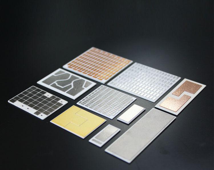
Engineering Solutions for DBC, DPC, and AMB Ceramic Substrates in Electric Mobility, Renewable Energy, Industrial Power Conversion, and Advanced Electronics
NMMech | Advanced Ceramic Solutions
Building Better Electronics Through Materials and Engineering
The next generation of electronic systems is being shaped by a common set of challenges: higher power density, more demanding thermal requirements, compact designs, and increasing expectations for long-term reliability. From electric vehicle inverters and industrial motor drives to renewable energy converters, LED modules, and advanced semiconductor packaging, electronic designers need materials that support efficient heat transfer, dependable electrical insulation, and stable performance under demanding operating conditions.
Advanced ceramic substrates play an important role in meeting these requirements. By combining the insulating properties of technical ceramics with engineered metal layers, ceramic circuit substrates provide a platform for integrating power semiconductor devices and other heat-sensitive electronic components.
At NMMech, we focus on ceramic substrate solutions designed around application requirements. Our technical discussions cover material selection, copper or metal-layer configuration, substrate dimensions, circuit patterns, and project-specific manufacturing considerations. The objective is to help customers identify a substrate solution that fits their design, assembly process, and performance targets.
A successful electronic system depends on more than an individual component. Matériaux, circuit design, bonding technology, assembly processes, cooling structures, and quality verification must work together. Understanding these relationships is the starting point for selecting the right ceramic substrate.
1. The Industry Challenges Behind Advanced Ceramic Substrate Solutions
Managing Heat in High-Power Electronics
Power semiconductor devices convert and control electrical energy, but some of that energy is released as heat. As power density increases and electronic packages become smaller, removing heat efficiently becomes more challenging.
Excessive operating temperature can affect semiconductor performance, accelerate material degradation, and place additional stress on solder joints and other interfaces. A well-designed thermal path is therefore essential to the overall reliability of power electronics.
Ceramic substrates can support heat transfer from semiconductor devices toward a baseplate, heat sink, or other cooling structure. The actual thermal performance depends on the ceramic material, layer thicknesses, interface materials, circuit layout, assembly quality, and cooling design. Selecting a substrate should therefore be part of the complete thermal-management strategy.
Maintaining Electrical Insulation
Many power electronic systems operate at elevated voltages and require reliable electrical separation between conductive regions and surrounding structures. The substrate must provide suitable insulation while supporting the required circuit configuration.
Technical ceramics are used in these applications because of their electrical insulating properties and their ability to function in demanding thermal environments. The appropriate ceramic material and thickness depend on the voltage requirement, geometry, operating environment, and applicable qualification criteria.
Electrical insulation must be evaluated within the finished assembly. Creepage distances, clearance distances, contamination, mounting conditions, and system-level design can all affect electrical safety.
Balancing Power Density, Size, and Reliability
Smaller electronic packages can reduce system volume and support more compact equipment, but they can also concentrate heat and increase mechanical or thermal stress. Engineers must balance thermal performance, isolation électrique, résistance mécanique, manufacturing tolerances, and cost.
Ceramic substrate technologies provide different design options for this balance. The most suitable choice depends on the target application, the required circuit pattern, the metal layer, the ceramic material, and the expected operating conditions.
 2. Our Ceramic Substrate Technology Portfolio
 2.
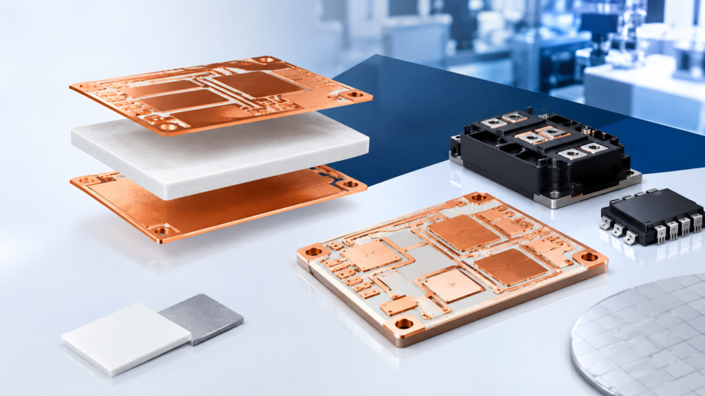
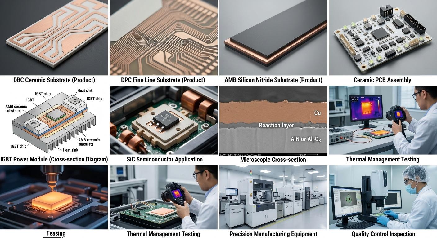
DBC, DPC, and AMB are established ceramic substrate technologies used in different electronic applications. Although all combine ceramic materials with conductive metal structures, they differ in their metallization or bonding methods and may be suited to different design requirements.
DBC — Direct Bonded Copper
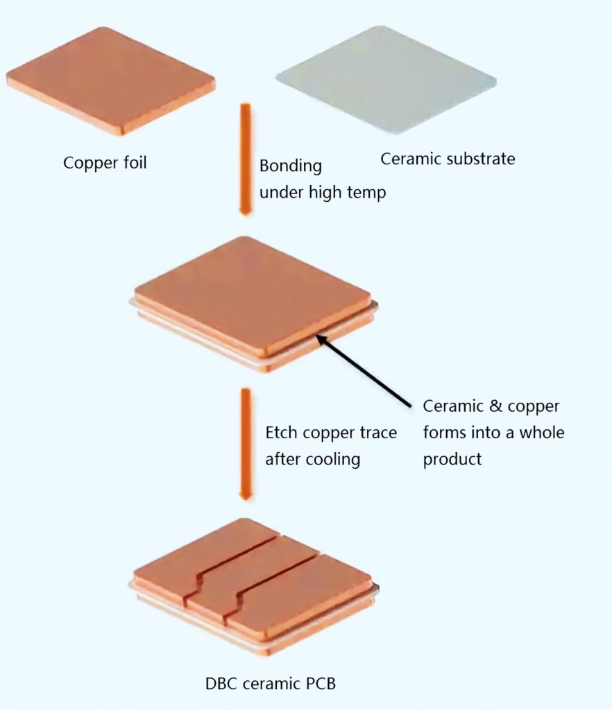
Cuivre à liaison directe (DBC) substrates use a controlled bonding process to join copper to a ceramic base, commonly alumina (Al₂O₃) or aluminum nitride (Aln).
DBC is frequently considered for power electronics because it can provide substantial copper conductor thickness, electrical insulation through the ceramic, and a useful thermal path. Depending on the design and process capability, DBC substrates can support circuit patterns for IGBT and SiC power modules, electric vehicle inverters, industrial drives, and power conversion equipment.
Key design considerations include copper thickness, ceramic material, substrate dimensions, circuit geometry, bond integrity, flatness, and the thermal and mechanical demands of the finished assembly.
DPC — Direct Plated Copper
Direct Plated Copper (DPC) is a ceramic metallization technology in which copper is deposited directly onto a ceramic substrate through a plating-based process. DPC can be useful for designs requiring relatively fine circuit features and precise metal patterns, depending on the material system and manufacturing capability.
Potential applications include LED packaging, optoelectronics, sensors, RF-related components, and selected electronic packages where circuit geometry and dimensional precision are important.
When evaluating DPC, designers should consider the required line width and spacing, copper thickness, ceramic material, surface finish, adhesion, and compatibility with die attachment or other assembly processes.
AMB — Active Metal Brazing
Active Metal Brazing (AMB) uses an active-metal brazing process to join copper and ceramic. AMB substrates are often evaluated for demanding power semiconductor applications where mechanical robustness, thermal performance, and resistance to repeated operating stresses are important.
AMB may be considered for selected high-power IGBT and SiC modules, electric mobility systems, and industrial power applications. Suitability depends on the ceramic material, copper configuration, brazing process, substrate geometry, and the requirements of the complete module.
How to Choose Between DBC, DPC, and AMB
There is no single substrate technology that is best for every application. A practical selection process considers the electrical, thermal, mechanical, manufacturing, and commercial requirements together.
For example, a design that prioritizes a robust copper circuit for a power module may evaluate DBC or AMB, while a design requiring finer circuit geometry may evaluate DPC. These are starting points for engineering discussion, not universal rules. Final selection should be based on verified specifications, process capability, and application testing.
 3. Key Application Markets
 3.
Electric Vehicles and e-Mobility
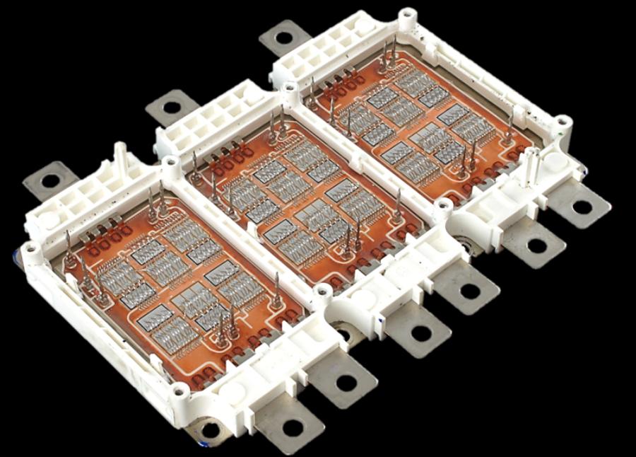
Electric vehicles rely on power electronics to convert and manage energy between the battery, motor, charging system, and other electrical subsystems. Traction inverters, onboard chargers, DC-DC converters, and related power modules must operate under demanding electrical and thermal conditions.
Ceramic substrates can help provide electrical insulation and thermal pathways in these assemblies. The material and substrate design should be evaluated alongside semiconductor selection, module architecture, cooling structure, vibration exposure, and expected thermal cycling.
For e-mobility projects, important design inputs include operating voltage, current, power losses, cooling requirements, substrate dimensions, copper thickness, and the qualification plan. Early coordination between substrate suppliers, module designers, and assembly teams can reduce design risks before volume production.
Renewable Energy and Power Conversion
Solar inverters, wind power converters, energy storage systems, and grid-related power electronics rely on semiconductor modules to control electrical energy. These systems may face changing loads, outdoor environmental conditions, and repeated thermal cycles.
Ceramic substrates can support insulation and heat transfer in power modules used in these systems. The final design must account for the expected operating profile, enclosure conditions, cooling method, service life, and applicable reliability requirements.
Industrial Motor Drives and Power Supplies
Industrial automation depends on variable-frequency drives, servo systems, high-power supplies, welding equipment, and other power conversion technologies. These systems may operate for long periods and experience repeated switching, thermal loading, and demanding production environments.
A properly specified ceramic substrate can contribute to a stable thermal and electrical design. Selection should account for current, switching conditions, operating temperature, package structure, and the assembly process.
 LED Packaging and Optoelectronics
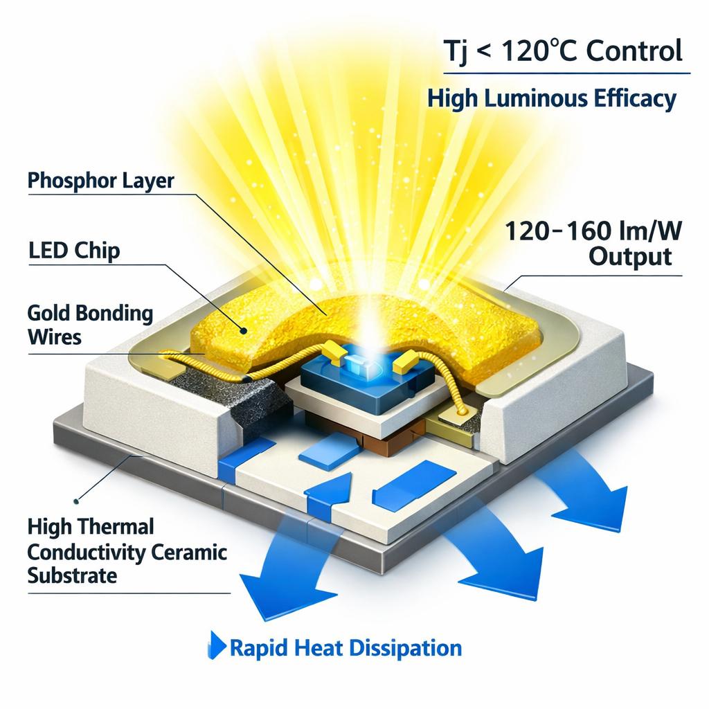
LED devices convert electrical energy into light, and thermal management is an important factor in maintaining optical performance and service life. Ceramic substrates can provide an insulating platform and a heat-transfer path for selected LED packages and high-power lighting applications.
DBC and DPC may be evaluated according to the required circuit geometry, thermal performance, copper thickness, package dimensions, and production process. The best option depends on the LED architecture and the manufacturer’s validated capabilities.
Semiconductor Packaging and Advanced Electronics
Power semiconductor packaging requires close coordination between the die, conductive patterns, insulating materials, attachment layers, and cooling structure. As device technologies evolve, including the wider use of silicon carbide, designers must consider switching performance, heat generation, insulation, and package reliability together.
Ceramic substrates can form part of this integrated design. Their performance should be assessed as part of the complete module rather than as an isolated material property.
Sensors, RF, and Specialized Electronic Assemblies
Selected sensors, RF-related components, and specialized electronic packages require a combination of circuit precision, insulation, dimensional control, and thermal stability. Depending on the design, ceramic-based circuit substrates may provide a suitable alternative to conventional organic materials.
The right solution depends on the frequency range, circuit geometry, electrical conditions, environmental requirements, and assembly method. Application-specific evaluation is essential before choosing a substrate technology.
4. From Application Challenge to Engineering Solution
A reliable substrate project begins with a clear understanding of the customer’s problem. Rather than choosing a material solely by name, the engineering process should identify the performance requirement that the substrate must satisfy.
Step 1: Define the Operating Conditions
The initial review should establish the intended application, electrical loading, operating temperature, thermal path, mechanical constraints, and expected service environment. These factors help determine which substrate technologies are worth evaluating.
Step 2: Review Materials and Structure
The next step is to consider ceramic material, ceramic thickness, metal-layer material, metal thickness, and whether the design requires single-sided or double-sided metallization. The structure should match both the electrical design and the thermal-management strategy.
Step 3: Evaluate Circuit Geometry
Circuit drawings, Gerber data, pad dimensions, line width, spacing, isolation distances, and dimensional tolerances should be reviewed for manufacturability. Early review can identify features that may require design adjustments.
Step 4: Align the Substrate With Assembly Requirements
A ceramic substrate does not operate independently. It must fit the die-attachment method, soldering process, baseplate, heat sink, and overall module construction. The customer and supplier should agree on relevant surface, flatness, dimensional, and inspection requirements.
Step 5: Validate Before Volume Production
Prototype samples can be used to assess dimensions, circuit quality, assembly compatibility, and application-specific performance. Where necessary, the qualification plan may include thermal cycling, power cycling, insulation tests, bond or adhesion evaluation, and other relevant tests.
Testing requirements should be agreed upon in advance. Not every application requires the same test package, and no single test can establish the reliability of an entire electronic system.
 5. Manufacturing Quality and Process Control
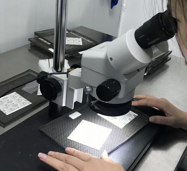 5.
Consistent product quality requires attention throughout the manufacturing process, from incoming materials to final inspection. Depending on the substrate technology, manufacturing may involve ceramic preparation, metallization or copper bonding, circuit patterning, etching or other pattern-forming steps, cleaning, dimensional inspection, and packaging.
Material Consistency
Variations in ceramic thickness, surface condition, copper thickness, and incoming material quality can affect downstream processing. Incoming inspection and material traceability help support consistent production and make investigations more effective if deviations occur.
Bonding and Metallization Quality
For DBC and AMB, the copper-to-ceramic interface is a critical consideration. For DPC, metallization quality, adhesion, and pattern definition are important. The appropriate inspection method depends on the technology, product design, and agreed specification.
Circuit Accuracy
Circuit dimensions must align with the design and manufacturing tolerances. Copper thickness and pattern geometry affect achievable line widths and spacing. The design should therefore be checked against the supplier’s validated manufacturing capability.
Cleanliness and Final Inspection
Residues and contamination can interfere with assembly and product performance. Appropriate cleaning, visual inspection, dimensional measurement, and electrical checks can help identify defects before shipment.
Documentation and Traceability
For projects with demanding quality requirements, agreed documentation may include material information, inspection results, lot identification, and relevant test reports. Clear specifications and traceability help customers and suppliers communicate consistently and investigate potential quality issues.
6. Reliability Is a System-Level Responsibility
A ceramic substrate is one part of a larger electronic assembly. Long-term performance also depends on semiconductor characteristics, die attachment, solder joints, baseplate design, thermal interface materials, cooling systems, mounting conditions, and operating profiles.
Thermal cycling can cause materials with different coefficients of thermal expansion to move differently. Mechanical vibration and mounting stress can also affect the assembly. The resulting stress distribution depends on the entire package design, not on one material parameter alone.
For this reason, substrate selection should be integrated into the module development process from an early stage. Design reviews, manufacturing capability checks, prototype assembly, and application-relevant qualification can help identify issues before mass production.
Reliability claims should be supported by appropriate test data and defined operating conditions. A substrate specification should state the relevant requirements rather than relying on broad statements such as “high reliability” without supporting criteria.
7. Customization and Engineering Collaboration
Different customers may need different ceramic materials, copper thicknesses, circuit geometries, dimensions, tolerances, and packaging arrangements. A useful supplier relationship begins with a technical review of the application and the customer’s drawing or preliminary design.
NMMech welcomes technical discussions about ceramic substrate projects, including DBC, DPC, and AMB requirements. Customers can share their intended application, material preference, copper configuration, dimensions, circuit layout, annual demand, and expected development schedule for an initial review.
When a project is still at the concept stage, available preliminary data can help clarify the key design questions. As the design develops, updated drawings and agreed acceptance criteria can support a more efficient sampling and validation process.
The goal is to establish a practical manufacturing solution that matches the product requirements and the supplier’s verified process capability.
8. Supporting the Journey From Prototype to Production
The transition from an engineering sample to repeat manufacturing requires more than a successful first article. It involves agreement on drawings, materials, tolerances, inspection methods, packaging, traceability, and change control.
During prototype evaluation, customers should confirm that the substrate can be assembled using the intended process and performs according to the agreed requirements. Any necessary design or process adjustments should be documented before production release.
For repeat orders, consistent material control and manufacturing records help maintain alignment with the approved design. If a change to material, process, or specification is proposed, the customer and supplier should evaluate its impact before implementation.
Clear communication at each stage helps reduce avoidable rework and supports a more predictable project schedule.
9. Why NMMech?
NMMech focuses on advanced ceramic substrate solutions for customers developing power electronics and other specialized electronic products. Our approach begins with the customer’s application and technical requirements rather than assuming that one substrate structure will suit every project.
We encourage customers to provide drawings, operating conditions, ceramic material preferences, metal-layer requirements, dimensions, and quality criteria. This information helps establish a more focused technical discussion and provides a foundation for reviewing potential manufacturing options.
For projects involving DBC, DPC, or AMB, material selection and substrate design should be aligned with the intended application, assembly method, and performance targets. The final specification should clearly identify the requirements that will be used for production and acceptance.
10. Build Your Next Ceramic Substrate Solution With NMMech
The development of reliable electronics depends on the integration of materials, design, manufacturing, and validation. Advanced ceramic substrates can help address important requirements in thermal management, isolation électrique, circuit integration, and package construction—but the best result comes from selecting the right technology for the complete application.
Whether your project involves electric vehicle power modules, industrial power conversion, renewable energy, LED packaging, or specialized electronics, early technical collaboration can help clarify material choices, circuit requirements, and manufacturing feasibility.
Contact NMMech to discuss your DBC, DPC, or AMB ceramic substrate project. Share your application, drawing, material preferences, technical specifications, and estimated demand to start a solution-focused engineering discussion.
#Advanced ceramic substrate solutions, #Substrat céramique DBC, #DPC ceramic substrate,# AMB ceramic substrate, #power electronics substrate,#IGBT substrate, #SiC power module substrate, #ceramic substrate for EV inverter, #ceramic substrate for LED packaging, #power module thermal management.
 DBC, DPC, AMB Ceramic Substrates and PCB Industry Resources
 DBC, DPC,
Explore authoritative standards organizations, semiconductor industry associations, academic research platforms, and technical resources related to DBC, DPC, and AMB ceramic substrates, ceramic PCBs, power electronics, and advanced electronic packaging.
These resources can help engineers, researchers, purchasing teams, and manufacturers learn more about ceramic substrate technologies, thermal management, isolation électrique, semiconductor packaging, and PCB manufacturing.
Technical Resources for Ceramic Substrates, PCB Technology and Power Electronics
Explore international technical organizations, research institutions,
academic publications, and engineering resources related to ceramic
substrates, electronic packaging, power semiconductor reliability,
thermal management, and printed circuit board technologies.
International Technical Organizations
IEEE Electronics Packaging Society
— Research and technical knowledge covering electronic packaging,
materials, thermal design, and reliability.
Institute of Electrical and Electronics Engineers
— International engineering research and professional knowledge
covering electronics and electrical engineering.
IPC International
— Industry standards, technical publications, and resources for
printed circuit boards and electronics manufacturing.
International Electrotechnical Commission
— International electrotechnical standardization and technical
information for electrical and electronic technologies.
SEMI
— Industry information and initiatives related to semiconductor
manufacturing and advanced electronics.
American Society of Mechanical Engineers
— Engineering knowledge relevant to thermal systems, mechanical
design, materials, and reliability.
Government Research and Scientific Institutions
National Institute of Standards and Technology
— Materials characterization, measurement science, and engineering
research.
U.S. Department of Energy: Electric Drive Systems Research
— Research on power electronics, electric-drive systems, advanced
packaging, and thermal management.
Advanced Research Projects Agency-Energy
— Research programs and technical initiatives addressing advanced
energy technologies and power systems.
Office of Scientific and Technical Information
— Scientific and technical publications from U.S. Department of
Energy research programs.
NASA
— Aerospace engineering, electronic systems, and high-reliability
technology research.
NASA Electronic Parts and Packaging Program
— Electronic parts assurance, packaging reliability, and
qualification-related technical information.
National Laboratory of the Rockies
— National laboratory research in energy systems and related
advanced engineering technologies.
National Renewable Energy Laboratory
— Research on renewable energy systems, power conversion, and
energy technology development.
Advanced Ceramics and Electronic Packaging Research
Fraunhofer Institute for Ceramic Technologies and Systems
— Research in technical ceramics, ceramic processing, and
ceramic-based electronic systems.
Fraunhofer IKTS: Rethink Power Electronics Research
— Research on functionalized ceramic DCB substrates and monitoring
technologies for power electronic modules.
Fraunhofer Institute for Reliability and Microintegration
— Electronic packaging, system integration, interconnection
technologies, and reliability research.
Fraunhofer Institute for Integrated Systems and Device Technology
— Semiconductor materials, power electronics, and device technology
research.
NC State Department of Materials Science and Engineering
— Academic research and education in materials science, ceramics,
and engineering materials.
American Ceramic Society
— Scientific and technical knowledge related to ceramic materials,
processing, properties, and applications.
Academic Literature and Research Databases
IEEE Xplore Digital Library
— Engineering papers on power electronics, electronic packaging,
semiconductor devices, and reliability.
PubMed
— Biomedical and life-science literature, useful for specialized
materials research in medical electronics.
PubMed Central
— Full-text scientific articles, including open-access materials
and engineering research.
ScienceDirect
— Scientific publications covering ceramics, material interfaces,
thermal management, et l’électronique de puissance.
SpringerLink
— Academic literature in materials science, applied physics,
electronics, and engineering.
Google Scholar
— Scholarly search for research on DBC, DPC, AMB, ceramic
substrates, and electronic packaging.
Matériaux
— Peer-reviewed research on materials science, ceramics,
interfaces, and material characterization.
Nature Portfolio
— Scientific research and reviews across materials science,
engineering, and related technology fields.
Direct Bonded Copper and Power Electronics Research
Characterization of Materials and Their Interfaces in a Direct Bonded Copper Substrate
— Research on copper, ceramic, and interface behavior in DBC
substrates for power electronics applications.
DBC Technology for Low Cost Power Electronic Substrate Manufacturing
— Research on DBC processing and ceramic-based power substrate
manufacturing.
Machine Learning Algorithms for Design Optimization of Ceramic DBC Substrates
— Research into DBC substrate design optimization, stress analysis,
and reliability.
Enhancing Thermal Reliability of Ceramic Substrates Using Lotus-Type Porous Copper
— Research on thermal reliability and structural design of
alumina-based DBC substrates.
Emerging Advanced Electronic Packaging Materials for Thermal Management in Power Electronics
— A review of advanced ceramic substrates, thermal interface
materials, and thermal management challenges in power electronics.
Embedded PCB and DBC-Integrated Design of GaN Power Modules
— Research on integrated PCB and DBC designs for improved
electrical and thermal performance.
About NMMech
NMMech focuses on the research, development, and manufacturing of
precision ceramic substrates, including Direct Bonded Copper (DBC)
and Direct Plated Copper (DPC) technologies. Our technical interests
include ceramic material selection, copper-to-ceramic interfaces,
circuit pattern design, thermal management, and electronic packaging.
We support customized substrate development based on project
specifications and application requirements.